
DIY Training Guide: Introduction
Learn how to use the eCADSTAR applications with the online DIY training. The training guides you through the process of creating a parts in a library, setting up the technology and design rules for a PCB project, creating the schematic for the project and then producing a PCB circuit, including analyzing the design and layout, using various features and functions of the eCADSTAR Applications.
The DIY Training Guide will familiarize you with the basic functionality of eCADSTAR by describing the application, and providing short, practical tasks. These tasks will guide you through using eCADSTAR Library Editor, including the Technology and Design Rule Editors, eCADSTAR Schematic Editor and eCADSTAR PCB Editor. They also provide training for SI Analysis, PI/EMI Analysis and SPICE Controller.
During the process of creating a PCB design, you will update the library, configure technologies and rules, and create a schematic. Each section of the training can be completed in any order, as the required data is provided. However, it is recommended that you follow the training in sequential order.
How to use Training
There are 4 main sections to the training, one for each of the eCADSTAR Applications.
- eCADSTAR Library Editor, including Technology and Design Rule Editors
- eCADSTAR Schematic Editor, including SPICE Controller
- eCADSTAR PCB Editor, including High Speed PCB Design
- eCADSTAR Analysis module, including Signal Integrity Analysis, Power Integrity/EMI Analysis and Electrical Editor.
The training is presented in the intended order of learning but you can choose which training you complete depending on which application/s you are going to use as part of your job role.
Within each section there will be various modules guiding you through the basic operation of that eCADSTAR application. You will be introduced to the application the features and functions, shown the user interface and controls and how to get started in that application. You will then be guided through the set-up, design and analysis process, following the typical process flow, using the files that are provided with your eCADSTAR installation.
Step-by-Step Guide
The DIY Training is your guide to getting started with the eCADSTAR tools.
It provides information to help you understand how the eCADSTAR applications work and guide you through using the basic features, along with tasks that provide a step-by-step guide on how to use the features and obtain the required results.
Each task has written steps with screen-shots to guide you through the task and a video visually guiding you through the task. You can choose to view the instructions or watch the video, or both, depending on how you wish to learn.
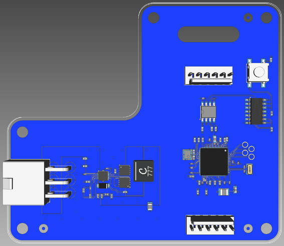
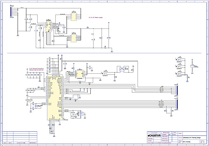
Figure 1: DIY Training PCB and Schematic Design
So, make yourself comfortable and get ready to delve into the world of eCADSTAR.
eCADSTAR Library Editor
Library Editor
Task 1: Using the Library Searcher
Optional Task: Creating New Libraries
Schematic Symbols
Task 2: Using eCADSTAR Symbol Editor
PCB Footprints
Task 3: Generating a Rectangular Pad
Task 4: Generating a Circular Pad
Task 7: Parametric Footprint Generation
Parts
Other Library Functions
Task 10 (Optional): Adding User-defined Attributes
Technology and Design Rules
Introduction
Technology and Design Rule Editors
Introduction to the Technology and Rule Libraries
The User Interface
Creating New Technology
Task 1: Opening the Technology Library
Task 2: Creating a Technology Library
User-Defined Layers
Task 3: Creating User Defined Layers
Layer Mapping
Task 4: Mapping the Footprint Layers to the PCB
Creating a Design Rule Library
Introducing the Design Rule Editor
Task 5: Building a Design Rule
Task 6: Setting the Track Specification
Task 7: Creating the Via Specification
Task 8: Setting the Conductor Clearances
Task 9: Configuring Hole/Area Settings
Task 10: Configuring Via Hole Settings
Task 1: Specifying Product and Application Settings
Task 11: Setting Component Areas
Task 12: Configuring Non Conductor Settings
Task 13: Configuring the Grids Tab
eCADSTAR Schematic Editor
Introduction
eCADSTAR Schematic Editor Introduction
eCADSTAR Schematic Editor Overview
eCADSTAR Schematic Editor Overview
Specifying Product and Application Settings
Task 1: Specifying Product and Application Settings
Creating a Schematic
Task 2: Creating a New Schematic
Task 3: Adding Parts and Symbols
Task 4: Adding and Naming Nets
Task 6: Grouping Components for Placement
Design Rule Checking and Parts Lists
Task 7 (Optional): Creating Variants
Task 8 (Optional): Specifying a User-defined Attribute
eCADSTAR PCB Editor
Introduction
eCADSTAR PCB Editor Introduction
The eCADSTAR PCB Editor Interface
PCB Generation
Display and Environment Settings
Task 2: Inputting the Board Outline
Task 3: Adding the Layout Area
Task 4: Entering Holes in the Board
Component Placement
Task 7: Placing Components by Coordinates
Task 8: Aligning Components by Location
PCB Routing
Positive Power Planes and Template Areas
Task 12: Creating Templates on Inner Layers
Task 13: Creating Templates on Outer Layers
Task 14: Adding Vias to a Design
Post Design Checking
PCB Cosmetics
Task 18: Creating Reference Designators (Symbol Mark Creation)
Task 21: Hole Drawing Creation
Manufacturing Outputs
Task 24: Producing a Parts List
The eCADSTAR PCB Autorouter
Introduction to the Autorouter
The Routing Strategy Dialog
Task 25: Adding an Unroute Row
Autorouter Tasks
Task 27: Applying Changes to the Strategy
The Routing Consultant
Task 28: Analyzing the Design and Correcting Issues
eCADSTAR High Speed PCB Design
Introduction to High Speed PCB Design
Design Entities for High Speed Design
Design Entities for High Speed Design
Task 2: Defining Differential Pairs
Topology Templates
Understanding Topology Templates
Task 3: Defining the Topology Templates
Task 4 (Optional): Defining the Topology Templates: Point-to-Point
Task 5: Assigning Topology Templates
Skew Groups
Task 7: Constraining Skew Groups
Routing to Constraints
Task 8: Routing Branched Address Signals
Task 9: Applying Batch Lengthening
Task 10: Applying Manual Lengthening
eCADSTAR Signal Integrity
Introduction to SI Analysis
Introduction to eCADSTAR SI Analysis
Task 1: Managing Simulation Models
Performing Post-Layout Analysis
Task 2: Performing Post-Layout Analysis
Defining the Layer Configuration
Checking the Topology
Task 3: Extracting the Topology
Task 4: Checking Transmission Lines
Performing Analysis
Task 5: Performing SI Analysis
Task 6: Performing Eye Pattern Analysis
Task 7: Performing TDR Analysis
Task 8: Performing FD Analysis
Checking in Constraint Browser
Task 9: Viewing Analysis Results
Task 10: Viewing a Summary of Differential Pairs
Task 12: Viewing a Pin Pair Route Report
Electrical Editor
Task 13: Performing What-if Analyses
Introduction to Electrical Editor
Placing a Termination Resistor
Analysis Result Viewer
Introduction to Analysis Result Viewer
Task 14: Using Analysis Result Viewer
eCADSTAR Power Integrity/EMI Analysis
Introduction
Introduction to eCADSTAR PI/EMI Analysis
Preparation for Analysis
Task 1: Preparation for Analysis
Recognizing and Changing the Component Type
Starting the PI/EMI Analysis Module
EMI Analysis
Task 2: Performing EMI Analysis
Verifying I/O Common Mode Noise
PI Analysis
Task 3: Performing PI Analysis
Checking Impedance Distribution
The Effects of a Decoupling Capacitor
DC Analysis
Task 4: DC Analysis
Setting the Supply and Consumption Source
Checking the Voltage Distribution
Checking the Current Distribution
eCADSTAR SPICE Controller
Introduction to Analog Simulation
LTspice Installation and eCADSTAR Configuration
Task 2: Setting the Executable Path in Schematic Application Settings
Task 3: Adding Include Files for the Simulation
Task 4: Setting Command-Line Arguments
SPICE Controller Tools and Settings
Component and Pin Properties for SPICE Simulation
Task 5a: Assigning a SPICE Model Name
Task 5b: Setting a SPICE Element Header
Task 5c: Assigning SPICE Pin Numbers
SPICE Controller Manager
SPICE Controller Manager Ribbon
SPICE Controller Tools in Schematic Editor
Task 6: Netlist Out to SPICE Controller
Task 7: Defining DC Voltage Sources
Task 8: Defining an AC Signal Source
Analysis Conditions
Performing LTspice Analysis
Using Numeric Values in SPICE Controller
Task 9: Creating a Transient Analysis
Task 10: Creating a DC Sweep Analysis
Task 11: Creating an AC Sweep Analysis
Task 12: Operating Voltage Point Display
Task 13: Using the Parameter Sweep
SPICE Controller Appendix
Task 15: Netlist Out (Automatic Voltage Generation)
