
Task 4: Mapping the Footprint Layers to the PCB
In this task, you will map the PCB layers to the relevant footprint layers, and add Symbol Mark layers.
- Select the Layer Configuration tab.
- Expand Conductor-1 using the arrow next to the layer name. All layers associated with Conductor 1 are shown.
- Right-click the Symbol mark-A layer, and select Add Symbol mark Layer. Symbol mark-A-1 and Symbol mark-B-1 are added.
Note
Both symbol mark layers are added because they must be balanced within the technology.
Both symbol mark layers are added because they must be balanced within the technology.
- In the Layer comment column for Symbol mark-A-1, type "Top Assembly" and press Enter.
- In the Layer comment column for Symbol mark-B-1, type "Bottom Assembly" and press Enter.
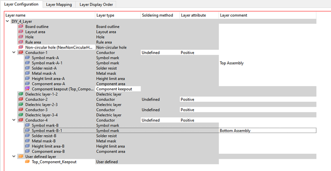
Figure 1: Layer Configuration
- Select the Layer Mapping tab.
- Click in the Side A column for Conductor-1, and select Top_Elec.
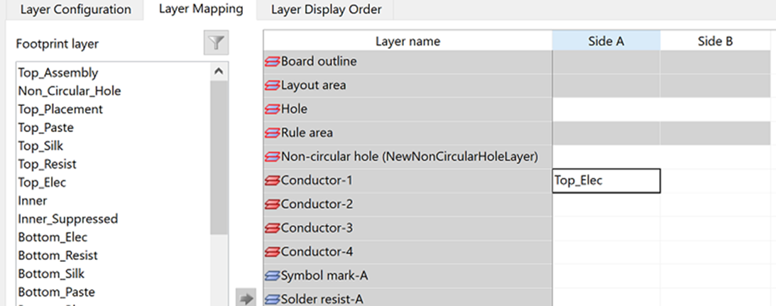
Figure 2: Layer Mapping for Side A
- Click in the Side B column for Conductor-1, and select Bottom_Elec. Footprint layers are mapped to board layers, using layer mapping. The swapping relationship is established between the top and bottom layers of the board.
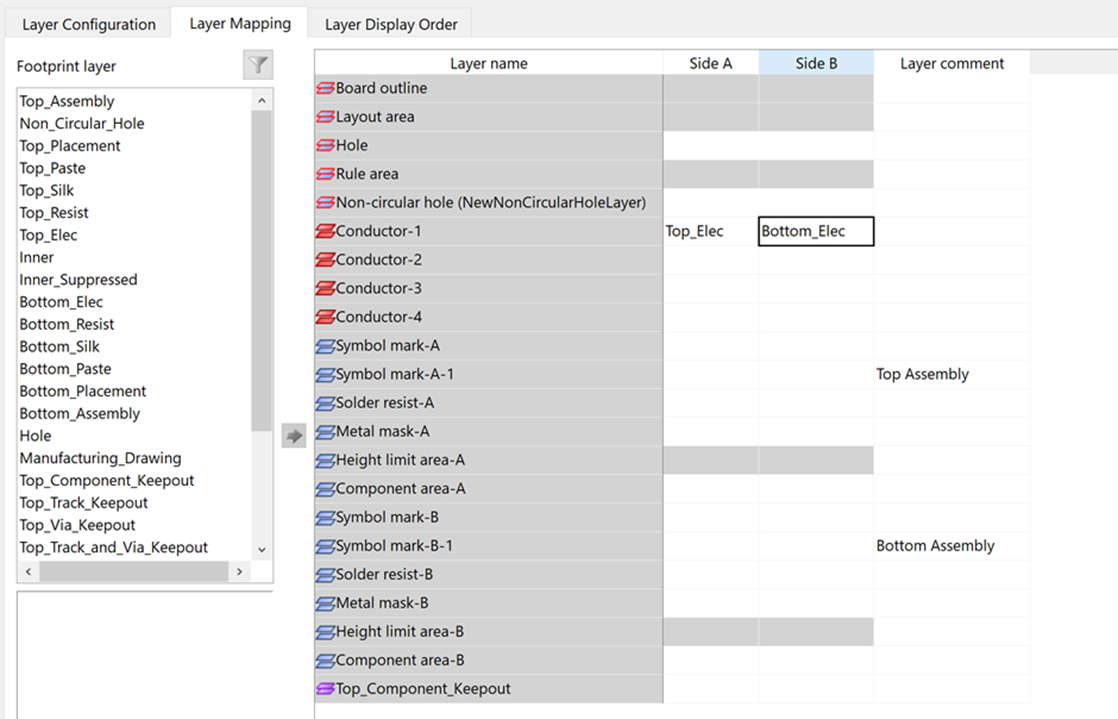
Figure 3: Layer Mapping for Side B
- Complete the assignment of layer information as shown in the image below.
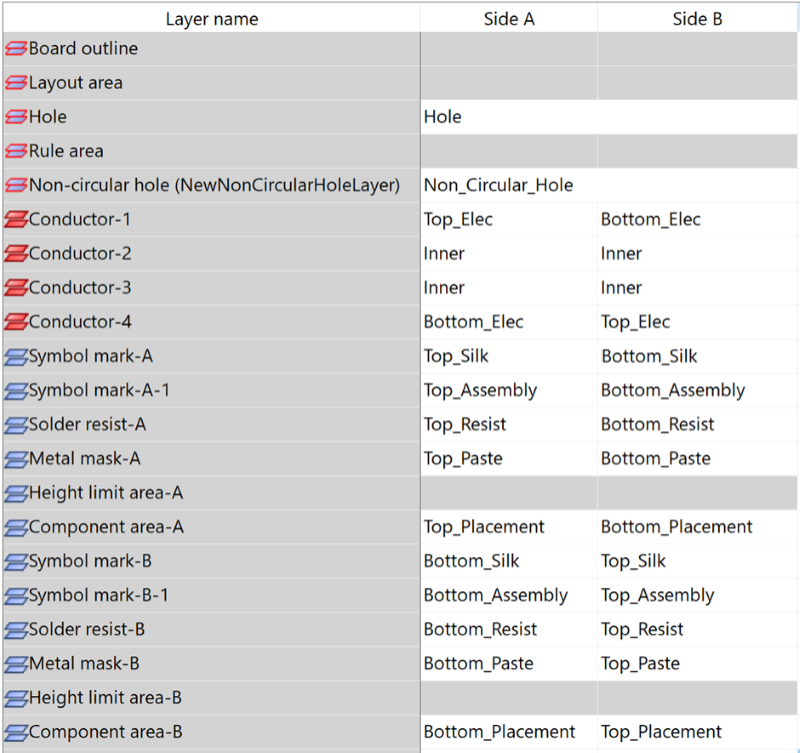
Figure 4: The Completed Technology File
- Save the technology by clicking File > Save on the ribbon. You have successfully mapped your library to the PCB Technology.
- Close the Technology Library tab in the eCADSTAR Library Editor.
This task is demonstrated in the following video.
