
Introducing the Design Rule Editor
In this section, you will explore the design rule libraries. Rule libraries contain a standard set of design rules, including the following:
- Board Parameters
- Layer Configuration
- Track Specifications
- Vias
- Differential Specifications
- Conductor Clearances
- Placement
- Non-conductor Clearances
- Grids
The image below shows the contents of a design rule library. This shows an 8-layer board. Your design is a 4-layer board, however.
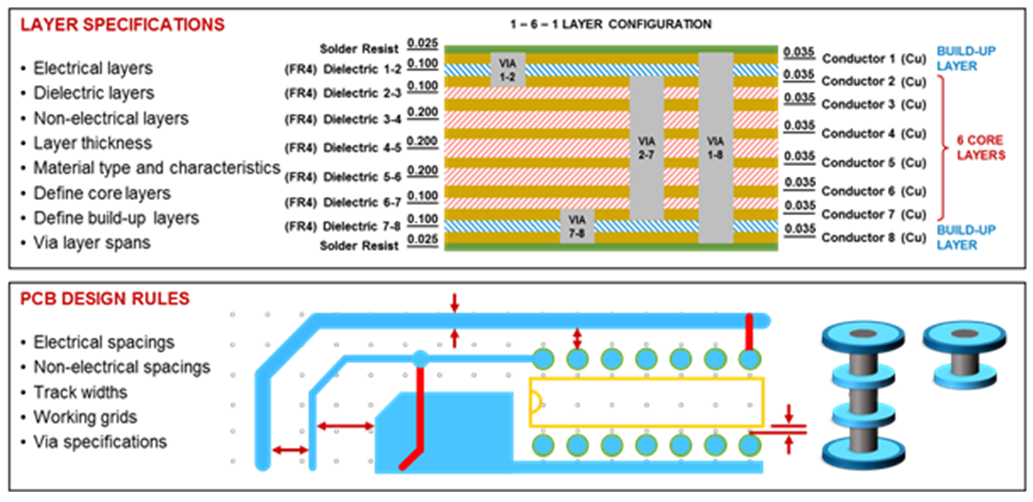
Figure 1 : Design Rule Library Contents
Introducing the Design Rule Editor GUI
You will now explore the Design Rule Editor. The following window is displayed when a design rule library is opened. The functions shown in each box are explained below.
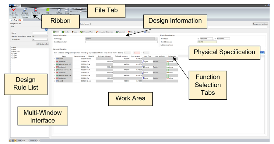
Figure 2: Design Rule Editor
File Tab
Operations on files and general application settings are provided.
Ribbon
The ribbon is a layered element consisting of tabs, groups and controls.
Design Rule List
This is used for listing current design rules and administering the design rule contents of the library. The following functions are available.
- Add
- Rename
- Delete
Multi-window interface
Multiple document tabs are located here.
Work Area
For the displaying and editing of design rule information.
Design Information
Assigned technology and board specification details.
Physical Specification
Maximum dimensions of the board, and specification of core and build up layers.
Function Selection Tabs
The various aspects of design rules which can be defined.
- Board
- Tracks
- Vias
- Differential Pairs
- Conductor Clearance
- Placement
- Non Conductor
- Grids
All tasks in this section of the DIY training are optional. The tasks to follow will instruct you to create a Design Rule similar to the supplied design rule titled 4_Layer. This design rule can be opened and viewed in the editor to help you understand the Design Rule Editor functionality.
