
Layer Mapping
In this section, you will explore layer mapping, before mapping the board technology layers with the footprint library layers, and adding user-defined layers. Layer mapping is the correlation between the generic layers that are used in the footprint library, known as footprint layers, with the physical board layers that are used in the PCB design, known as board layers. Mapping determines the board layer onto which padstacks, lines and other in-component objects are added. The following diagram shows an example of through-hole layer mapping.
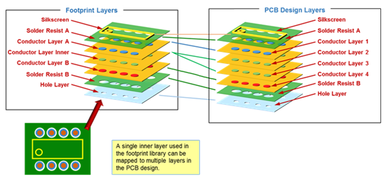
Figure 1: Through-Hole Layer Mapping
The library layers are defined in the DIY Library training course. For further information, refer to this document.
An example of Surface-Mount Layer Mapping is shown below:
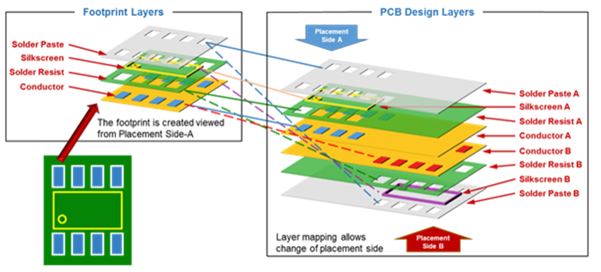
Figure 2: Surface-Mount Layer Mapping
Footprint Layer
Footprints are the visual representation of the part to be placed on your layout. They are constructed of:
- Solder Paste (for surface mount footprints)
- Outlines (symbol mark / assembly)
- Solder Resist
- Conductor
- Holes (for plated through-hole footprints)
PCB Design Layer
This is an actual process layer or documentation layer in the PCB design. These include conductive layers, drill layers, symbol mark, solder mask and solder paste layers. Additionally, various keep-outs, design rule enabling layers, and user-defined layers such as documentation can be included.
