
Task 5: Generating Padstacks
A padstack is a component’s interface to the board. For a single layer board, the layout will require one set of pads with holes for a Plated Through-Hole (PTH) component. For a multilayer board, a more complex arrangement of pads is required, with each pad being assigned to one or more footprint layers. Some examples of padstacks are shown below.
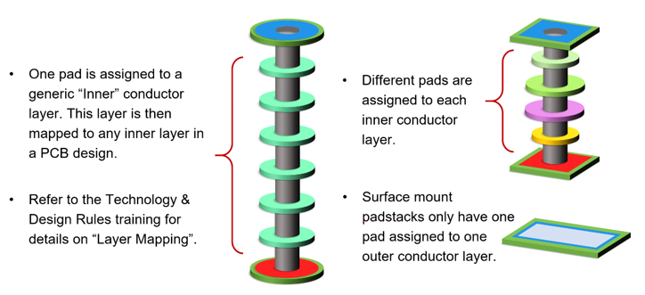
Figure 1: Padstack Examples
- It is recommended that the footprint library is kept simple, with only the minimum required number of layers defined. This allows a "one-to-many" assignment of pads for inner conductor layers.
- Individual pads can be assigned per conductor
layer, but this may increase the time required for library maintenance.
Generating a Plated Through-Hole (PTH) Padstack
In this task, you will create a Plated Through-Hole (PTH) padstack using the pads that were built in the last task. You will use this padstack in later tasks when building footprints.
- On the eCADSTAR Library Editor ribbon, click Home > Editors > Padstack. The Padstack Editor dialog is displayed.
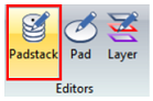
Figure 2: Opening the Padstack Editor
- In the Padstack Editor dialog, click Add Padstack. "NewPadstack-1" is created.
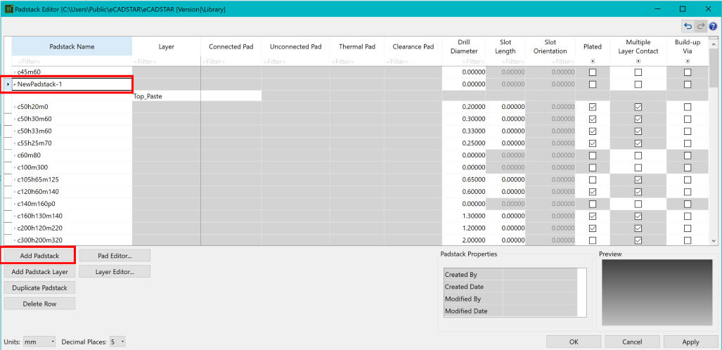
Figure 3: Adding a Padstack
- In the Padstack Name column, change the name of the padstack to "DIY-c200h120m220". This name represents a 2mm circle, with a hole of 1.2mm and a mask of 2.2mm.
- In the Drill diameter column, change the value to "1.200". The Multiple Layer Contact column becomes non editable and the check box is set.
- In the Slot Length column, leave the value at "0.000".
- In the Plated column, select the check box.
- In the Build-up Via column, ensure this check box is deselected. This completes the general parameter settings for the padstack.
- To set the first layer's parameter settings, in the Layer column, select Top_Resist.
- In the Connected Pad column, select DIY-c220.

Figure 4: Configuring the Padstack Editor
Adding a Padstack Layer
- In the Padstack Editor dialog, select the newly-built padstack, and click Add Padstack Layer.
- For the new layer, select Top_Elec in the Layer column.
- In the Connected Pad column, select DIY-c200.
- In the Unconnected Pad column, select DIY-c200.
- In the Thermal Pad column, select DIY-tc200.
- In the Clearance Pad column, select DIY-c220.
Adding a Second Padstack Layer
- In the Padstack Editor dialog, click Add Padstack Layer to add a second layer.
- For the new layer, select Bottom_Resist in the Layer column.
- In the Connected Pad column, select DIY-c220.
Adding a Third Padstack Layer
- In the Padstack Editor dialog, click Add Padstack Layer to add a third layer.
- For the new layer, select Bottom_Elec in the Layer column.
- In the Connected Pad column, select DIY-c200.
- In the Unconnected Pad column, select DIY-c200.
- In the Thermal Pad column, select DIY-tc200.
- In the Clearance Pad column, select DIY-c220.
Adding a Fourth Padstack Layer
- In the Padstack Editor dialog, click Add Padstack Layer to add a fourth layer.
- For the new layer, select Inner in the Layer column.
- In the Connected Pad column, select DIY-c200.
- In the Unconnected Pad column, select DIY-c200.
Leaving this cell empty will allow pad suppression to occur automatically within the PCB Editor. When a padstack has track or copper area connected, it will display the Connected Pad. When there is no track or no copper area connected, it will display the Unconnected Pad.
- In the Thermal Pad column, select DIY-tc200.
- In the Clearance Pad column, select DIY-c220.
- In the Padstack Editor dialog, click OK.
- In the displayed dialog, click Yes to accept changes.
Note that the newly-created layers are not ordered correctly. Close, and then re-open the Padstack Editor dialog to display the layers in the correct order, as shown below.
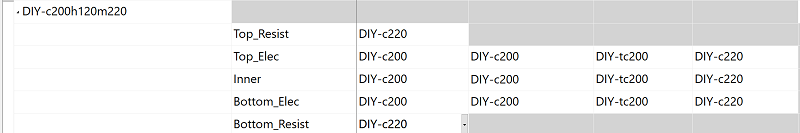
Figure 5: Re-Ordering Layers
This procedure is demonstrated in the following video.
Generating a Padstack for a Surface Mount Device (SMD)
In this task, you will create a Surface Mount Device (SMD) padstack using the pads that you created in task 3. You will use these in later tasks when building footprints.
- On the eCADSTAR Library Editor ribbon, click Home > Editors > Padstack. The Padstack Editor dialog is displayed.
- Follow the instructions in the previous task in this topic, but make the following changes:
- Change the name of the padstack to "DIY-r207_66m227_86".
- Only add the layers Top_Elec, Top_Paste and Top-Resist.
- In the Drill Diameter column, specify a value of "0.000".
The completed padstack parameters are shown below.

Figure 6: The Completed Padstack
This procedure is demonstrated in the following video.
