
Task 6: Creating a Footprint
In this task you will create the footprint for a 14 pin Small Outline Integrated Circuit (SOIC). This footprint will be used to continue building the Quad NAND gate CD4093BM96.
Unlike the other eCADSTAR tools, there is no direct way to open the Footprint Editor. To open it, either open an existing footprint from eCADSTAR Library Editor, or add a new footprint which you can then edit in Footprint Editor.
Placing Padstacks and Assigning Pin Numbers
- In eCADSTAR Library Editor, select the Footprints tab.
- On the eCADSTAR Library Editor ribbon, click Home > Rows > Add.
- In the Footprints tab, Footprint Name column, change the footprint name to "DIY_SO14".
- Select the "DIY_SO14" footprint, and click Home > Edit > Footprint to launch Footprint Editor as shown below.
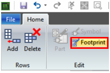
Figure 1: Opening the Footprint Editor.
- In the displayed Warning dialog, click Yes. Footprint Editor is launched.
- If the Pins panel is not displayed in Footprint Editor, then click View > Display > Pins on the ribbon. The Pins panel is displayed.
- In the Pins panel, Number of pins box, specify "14" and press Enter.
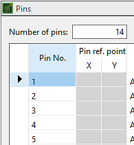
Figure 2: Setting the Number of Pins.
You can specify details for the font used for pin numbers and pin reference points, and the color of error marks, in the Application Settings dialog. To display this dialog, click File > Configuration > Application Settings on the main menu. Select the Canvas Information section.
- On the Status Bar click the Snap Grid split button, and select Grid Setting.
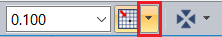
Figure 3: Snap Grid split button.
- In the Grid Settings dialog, set X pitch to “1.270” and set Y pitch to “2.425”. Close the dialog.
- On the Footprint Editor ribbon, click Footprint > Padstack/Pad > Padstack. The Padstack dialog is displayed.
- In the Padstack dialog, Padstack name box, select DIY-r207_66m227_86.
- In the Angle box, change the value to "90.000". The selected padstack attaches to the cursor.
- Place a padstack at X=”0.000” and Y=”2.425”. Then place three padstacks to the left, one grid pitch at a time, and a further three padstacks to the right of the original padstack, one grid pitch at a time.
- Place a padstack at X=”0.000” and Y=”-2.425”. Then place three padstacks to the left, one grid pitch at a time, and a further three padstacks to the right of the original padstack, one grid pitch at a time.
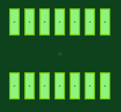
Figure 4: Placing the Remainder of the Padstacks.
- On Footprint Editor ribbon, click View > Canvas > Canvas View Settings. The Canvas View Settings dialog is displayed.
- In the Canvas View Settings dialog, Information tab, select Pin number. This setting will enable pin numbers to be displayed on the canvas.
- Close the Canvas View Settings dialog.
- On the Footprint Editor ribbon, click Home > Pin Settings > All. The Pin Settings (All) dialog is displayed.
- Select Entire area,
and set Pattern to
 Counter-clockwise
(BL).
Counter-clockwise
(BL). - Ensure that Start number and Digits are set to “1”.
- Click Execute. All padstacks are assigned a pin number.
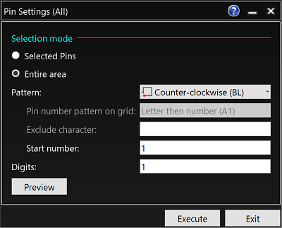
Figure 5: The Pin Settings (All) command.
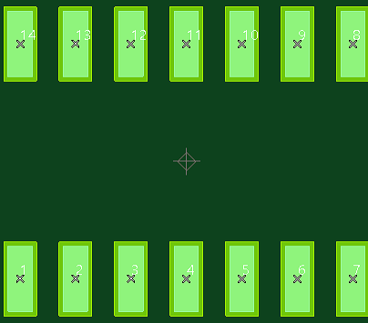
Figure 6: Padstacks with Pin numbers.
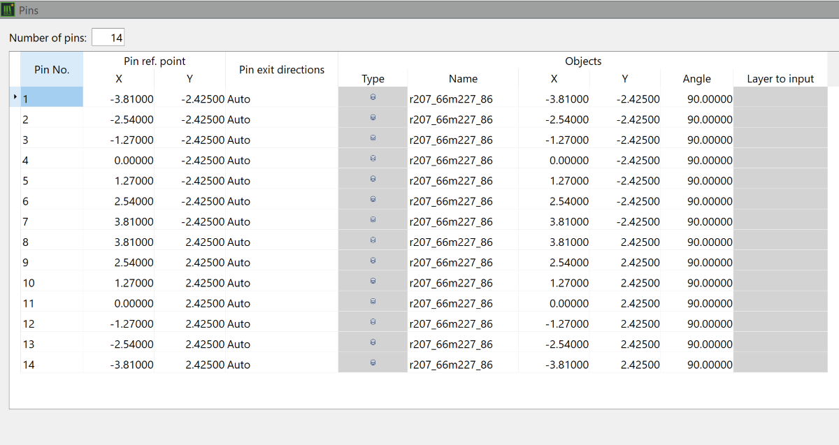
Figure 7: The Completed Pins Table.
- On the Status Bar, click the Snap Grid split button and select Grid Settings.
- In the Grid Settings dialog, set the X and Y pitch to “0.100”.
- Close the Grid Settings dialog.
This procedure is demonstrated in the following video.
Adding a Component Outline
- On the Footprint Editor ribbon, click View > Display > Layer Settings. Alternatively, click the Layer Settings button on the Status Bar. The Layer Settings panel is displayed.

Figure 8: Opening the Layer Settings Panel.
- On the Layer Settings panel, set the Active layer to Top_Silk using the radio button, as shown below. The Active layer is always visible.
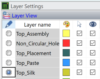
Figure 9: Setting the Layers.
- On the Footprint Editor ribbon, click Draw > Shapes > Polyline. The Line (Polyline) dialog is displayed.
- In the Line (Polyline) dialog, specify the values shown below.
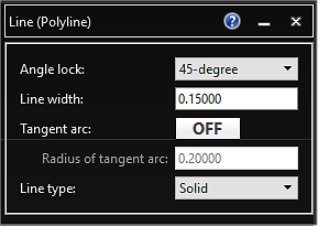
Figure 10: Setting the Line Width.
- Right-click on the canvas and select Input Coordinate on the assist menu. The Input Coordinate dialog is displayed.
- In the Input Coordinate dialog, Mode box, select Absolute.
- In the Input Coordinate dialog, specify the coordinates shown below and click Apply. The start point of your symbol mark now appears to the left side of pin 1.

Figure 11: Specifying absolute coordinates.
- In the Input Coordinate dialog, specify the coordinates shown below and click Apply.
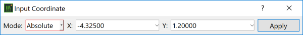
Figure 12: Specifying further absolute coordinates.
- Right-click the canvas and select Finish on the assist menu.
- On the Footprint Editor ribbon, click Home > Duplicate > Move. The Duplicate (Move) dialog is displayed. Select the polyline.
- In the Input Coordinate dialog, Mode box, select Relative and specify the coordinates shown below and click Apply. Close the command and Input Coordinate dialog.
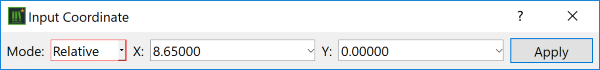
Figure 13: Specifying relative coordinates.
- The component outline is displayed as shown below.
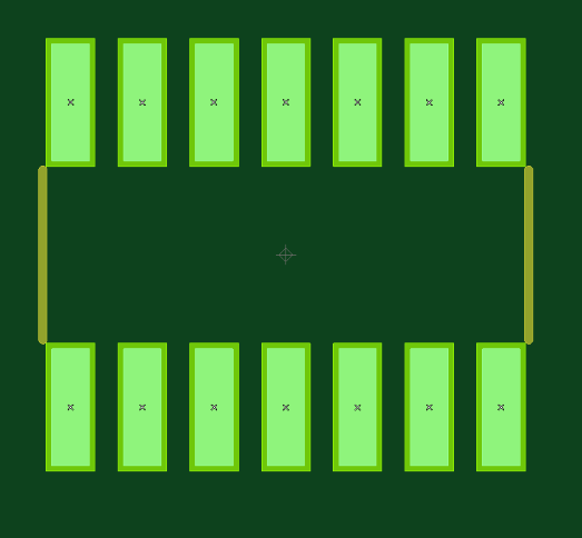
Figure 14: Symbol Mark.
To avoid compromising padstacks, ensure that silk screen layers do not overlap them.
This procedure is demonstrated in the following video.
Adding a Pin 1 Reference Point on the Top Silk Layer
- On the Status Bar, confirm that the following Snap Grid value is set.
Figure 15: Snap Grid split button.
- On the Footprint Editor ribbon, click Draw > Shapes > Circle. The Line (Circle) dialog is displayed.
- Click to start a circle at location X=”-4.600” Y=”-2.000”.
- Create a circle with a chosen diameter by dragging the cursor one grid point to the right. Click the canvas to finish.
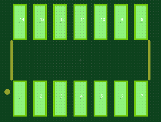
Figure 16: The Complete Symbol Mark Showing the Pin 1 Marker.
This procedure is demonstrated in the following video.
Adding the Assembly Outline
Using similar methods to those described above, create the assembly outline for the footprint. The assembly outline should be created on the Top_Assembly layer.
The assembly outline can be defined to show more details of the component. This allows more accurate documentation to be generated for the manufacturing process.
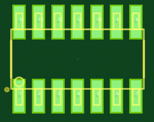
Figure 17: The Component Outline.
This procedure is demonstrated in the following video.
Adding the Placement Outline
- Change the Active Layer to Top_Placement.
- On the Footprint Editor ribbon, click Shape > Area Fill> Rectangle. The Area Fill (Rectangle) dialog is displayed.
- In the Area Fill(Rectangle) dialog, set the values shown below

Figure 18: Component Area (Rectangle) Settings.
- On the Status Bar, click the Snap Grid split button and select Grid Setting.
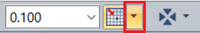
Figure 19: Snap Grid split button
- In the Grid Settings dialog, set the X pitch to “0.05” and set the Y pitch to “0.05”. Close the dialog.
- Draw a rectangular area by clicking on the canvas from X=”-4.450”, Y=”2.000” to X=”4.450”, Y=”-2.000”.
- Draw a second rectangular area by clicking on the canvas from X=”-4.300”, Y=”3.600” to X=”4.300”, Y=”-3.600”. Set the Height (Standoff - Maximum) value to "0.00000", as shown below.
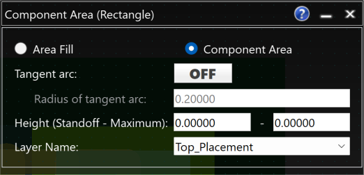
Figure 20: Component Area (Rectangle) Settings
The placement outline is added as shown below.
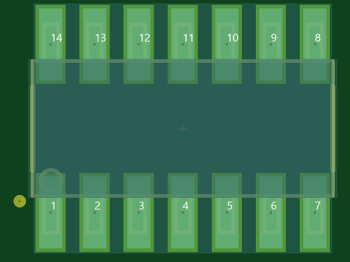
Figure 21: The Completed Placement Outline.
- Save and close the footprint.
This procedure is demonstrated in the following video.
- This component area represents the physical bounds of the component in 3D when placed into a PCB design. This shape will be used for DRC and collision checks in the PCB Editor.
- Standoff height and maximum height can be specified. The standoff height is the distance that components in the component area sit above the board surface. Maximum height is the maximum height of the components
- For through-hole components, component areas can be positioned on the reverse side to represent the protrusion of pins through the board.
- If component areas are not defined within the footprint, then when the items are added to the PCB design, an automatic component area is added to the footprint. For a through-hole component this will be on both the top and bottom placement layers. A rectangular bounding box is generated around all the design objects in the footprint on the top and/or bottom placement layers.
- For example, the footprint MOLEX_0022272061 (N) in the installed library would have the following.
- Top Placement layer: a rectangle around the extremes of the silkscreen or assembly shapes.
- Bottom Placement layer: a rectangle around the extremes of the six padstacks.
- As a further example, the footprint TP140 (N) in the installed library would have the following.
- Top Placement layer: a square around the extremes of the diameter of the silkscreen or assembly shapes.
