Task 7: Parametric Footprint Generation
In this task, you will generate a footprint for the MOLEX_0022272061 Plated Through-Hole (PTH) connector. You will use the Parametric Generation command this time, rather than generate the footprint manually.
- In eCADSTAR Library Editor, select the Footprints tab.
- On the eCADSTAR Library Editor ribbon, click Home > Rows > Add. A new row, named "NewFootprint-1", is added in the Footprints tab.
- Click on "NewFootprint-1" and change it to "DIY_CONN6".
- Right-click DIY_CONN6, and select Edit Footprint on the assist menu.
- In the displayed Warning dialog, click Yes. The Footprint Editor is launched.
- On the Footprint Editor ribbon, click Footprint > Generate > Parametric split button > Connector/ZIP. The Parametric Generation (Connector/ZIP) dialog is displayed.
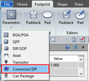
Figure 1: Selecting Connector/ZIP
- In the Parametric Generation (Connector/ZIP) dialog, select the Pin Shape tab.
- In the Pin count settings section, enter the following parameters to define the shape dimensions.
- Pin count m: 6
- Pin count n: 1
- Pin pitch W: 2.540
- Pin pitch L: 0.000
- Pin angle: 0.000
- In the Padstack Name box, load the padstack DIY-c200h120m220 that you created earlier.
- In the Position box, select Center.
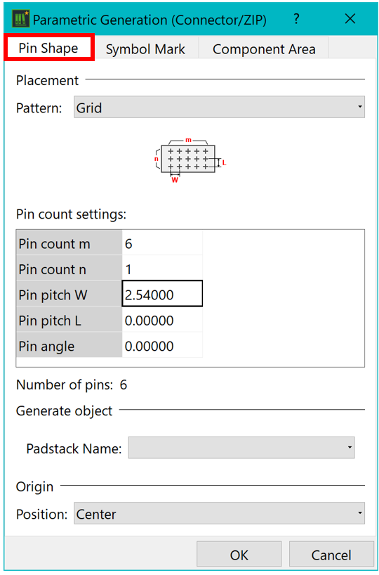
Figure 2: Setting Pin Shape Parameters
- Select the Symbol Mark tab and set the parameters shown below.
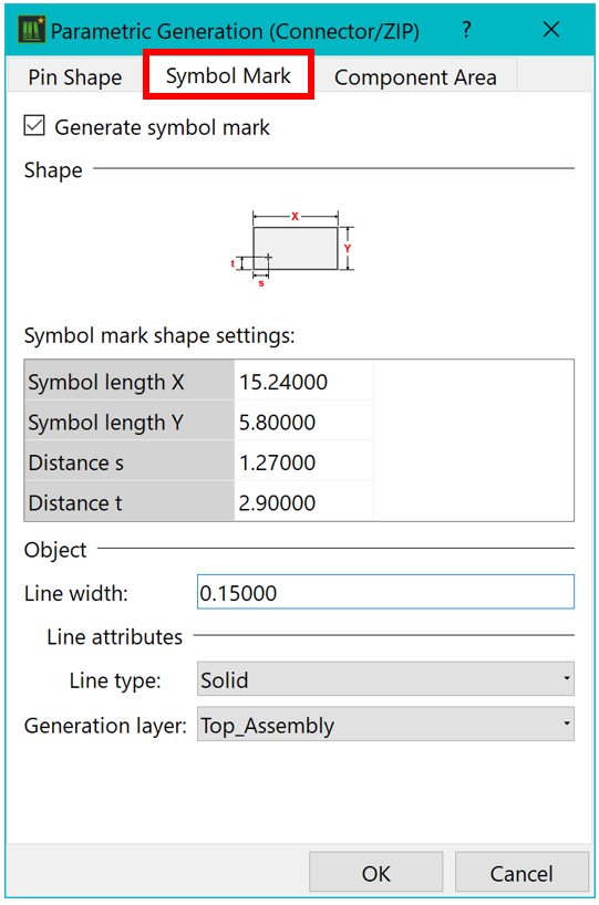
Figure 3: Setting Symbol Mark Parameters
- Select the Component Area tab, and set the parameters shown below.
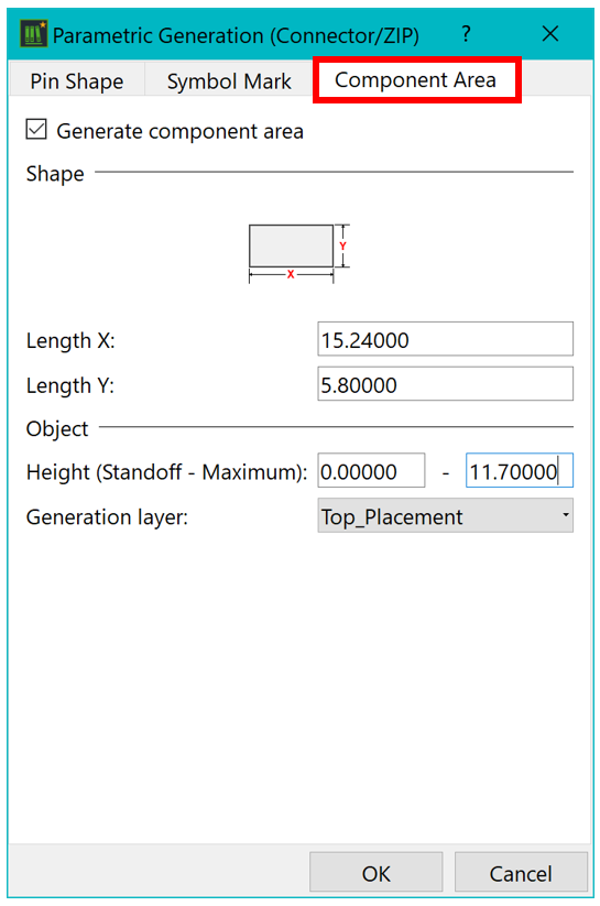
Figure 4: Setting Component Area Parameters
- Click OK in the Parametric Generation (Connector/ZIP) dialog.
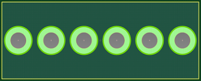
Figure 5: The Generated Footprint
- Using the previously-described methods, ensure the Top_Silk shape and orientation markers are added to the footprint, and padstacks are assigned Pins. When completed, the footprint should look similar to the image shown below.
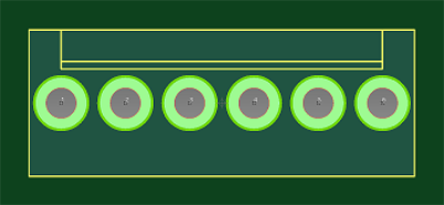
Figure 6: The Completed Footprint
- Save and Close the Footprint.
This task is demonstrated in the following video.

