
Task 9: Configuring Hole/Area Settings
In this task, you will learn how to configure the hole and area settings. General clearances for holes to other objects can be set, and clearances from electrical objects to layout and keepout areas.
-
In the Conductor Clearance tab select the Hole/Area tab, as shown below.

Figure 1: Hole Area Settings
- In the Design rule group section, create a design rule unit of "0.1mm" and click Add.
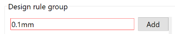
Figure 2: Design rule group
- In the Design rule group section, enter "0.10000" in the first cell of the Hole row, (also the first cell of the Track column).
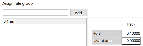
Figure 3: Design rule group spacings
- Copy the contents of this cell (first cell of the Hole row/Track column) by pressing Ctrl+C.
- Click on the arrow next to the Track row and drag the cursor down to the Area Fill row, to select all the cells in these two rows. Press Ctrl+V to paste the "0.10000" value into all selected cells.
- In the Design rule stack section, create an entry of "0.1mm" and click Add.
- In the Design rule stack section, select "0.1mm" in the Design rule group column for each conductor layer. The design rule stack is now ready to use.
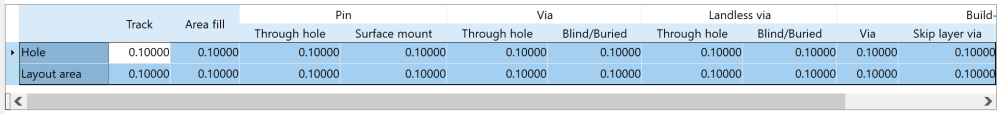
Figure 4: Design rule group spacings
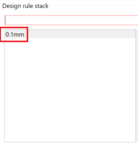
Figure 5: Design rule stack
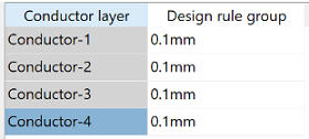
Figure 6: Setting Design rule group Values
- In the Default design rule stack box, select 0.1mm.
- On the ribbon, click File
> Save. At this stage, ignore any warnings or errors.
This task is demonstrated in the following video.
