
Task 14: Adding Vias to a Design
Using the Padstack command, it is possible to add vias into a design and connect them to flooded areas. In this task, you will set up a via size and span, and make connections to flooded planes.
- On the Padstack tab, click Padstack. The Padstack dialog is displayed.
- Set the active layer to Conductor-1.
- Set the parameters shown below.
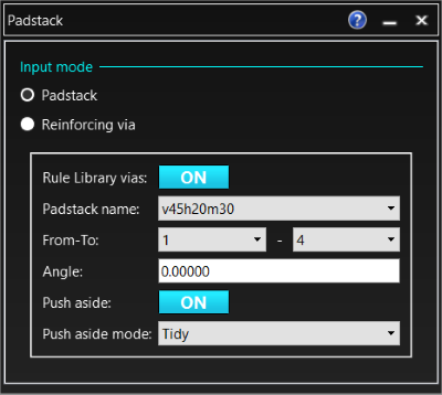
Figure 1: Padstack Settings
From the Padstack name pull down list, select the larger-sized via "v80h50m60" to add larger padstacks where larger space is available.
- Frame view the area below IC4, the 65 pin device.
- On the status bar, click
 Layer
Settings to display the Layer Settings
panel.
Layer
Settings to display the Layer Settings
panel. - In the Layer Settings
panel, ensure that only the Conductor-1
and Conductor-4 layers are visible
by selecting the
 Visible
layer check box for just these layers.
Visible
layer check box for just these layers. - With the via attached to the cursor, move over the flooded area and then right-click and select Specify Net on the assist menu.
- Click the GND0V flooded area. GND0V is now shown next to the via attached to the cursor.
- Click to place the via.
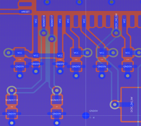
Figure 2: Adding a Via
- Repeat as necessary to place vias near to GND0V pins on components.
- Select the larger of the vias from the Padstack name box.
- Frame the area showing both the topside VIN_12V flooded areas, shown below.
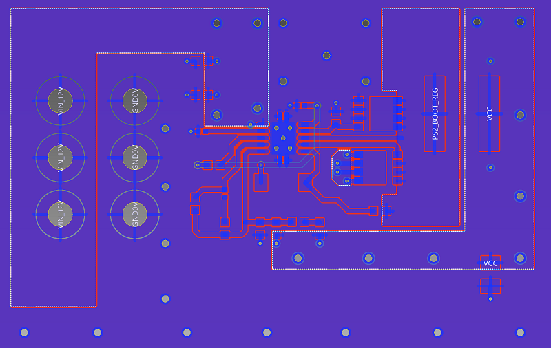
Figure 3: Via Pattern
- Add the larger vias to the flooded areas as shown.
To complete your design, a polygon area fill needs to be added on Conductor-3. This connects the two VIN_12V flooded areas. Do this by following the instructions in Task 12.
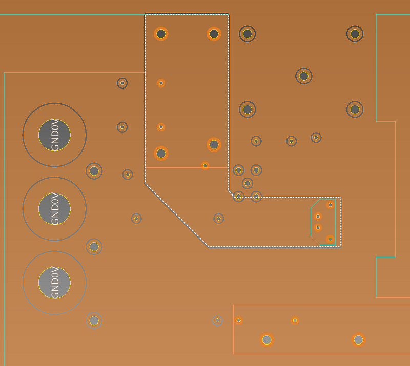
Figure 4: Polygon Area Fill
This task is demonstrated in the following video.
You will now learn about post routing processes.
