
Board Generation
In this section, you will generate an initial design. You will also learn how to create a 4-layer board for this training course, and how to view the various layers, and configure grids. You will set up the mouse and shortcut keys to your own preferences.
Task 1: Board Generation
In this task you will create a new design by specifying the design parameters.
- On the eCADSTAR PCB Editor ribbon, select File > Configuration > Product Settings.
- In the Product Settings dialog, set the library path shown below.
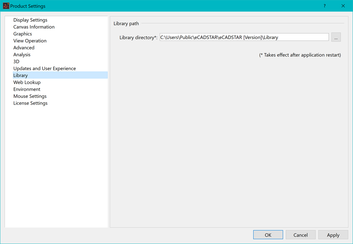
Figure 1: Setting the Library Path
- On the File tab, click New. The New (Design Data) dialog is displayed.
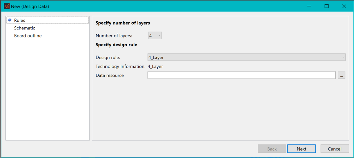
Figure 2: The New (Design Data) dialog.
- Specify "4" in the Number of layers box. Notice that this preloads design rule and technology file options based on a 4-layer PCB.
There could be many design rule and technology files with four layers, depending on the manufacturing process and layer stack-up. The creation of technology and rule files is covered in the Technology and Design Rule Editors training guide.
- Select the design rule “4_Layer” in the Design rule box. The dialog should be as shown below.
Figure 3: Specifying the Number of Layers
- Click Next.
- Click the Schematic radio button for the option to specify the directory of the relevant schematic design.
- Click the
 button to open an explorer window.
 - Browse to C:\Users\Public\eCADSTAR\eCADSTAR [version]\Designs\DIY_Training\SCH\DIY_Training\DIY_Training.sdes, and click Open.
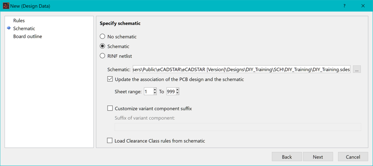
Figure 4: Specifying the Schematic Path
- Click Next. You can now create a board outline or copy one from another PCB design.
- Select Width/Height in the Creation method box.
- Enter a width and height of “150”
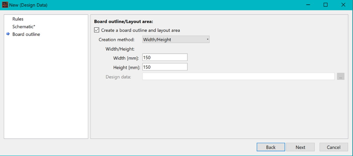
Figure 5: Specifying the Board Size
- Click Next. A summary of the settings is displayed. This allows you to go back to make any changes, if necessary.
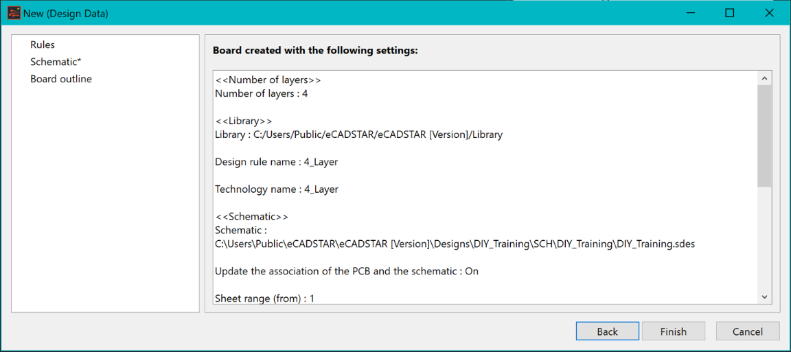
Figure 6: The board summary
- Click Finish. The board outline is created with components arranged above the board outline as shown below.
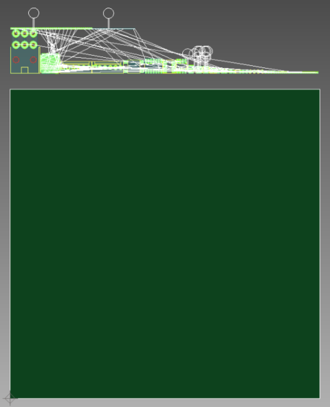
Figure 7: The Completed Board Outline
-
Save the design to the location: C:\Users\Public\eCADSTAR\eCADSTAR [version]\Designs\DIY_Training\PCB\MyDesign1.pdes. You will use this design later in the course.
This task is demonstrated in the following video.
You have now created a basic PCB. You will explore the display and environment settings next.
