
PCB Technology View
The PCB Technology View command provides a visual, scaled representation of a cross-section of the board. This is produced using board configuration information.
Operation Basics
Launch the PCB Technology View command as follows.
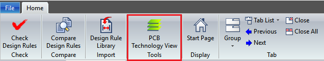
Figure 1: Launching the PCB Technology View command
The PCB Technology View dialog is displayed, as shown below. Resist thickness, conductor thickness, dielectric thickness and via definitions are displayed.
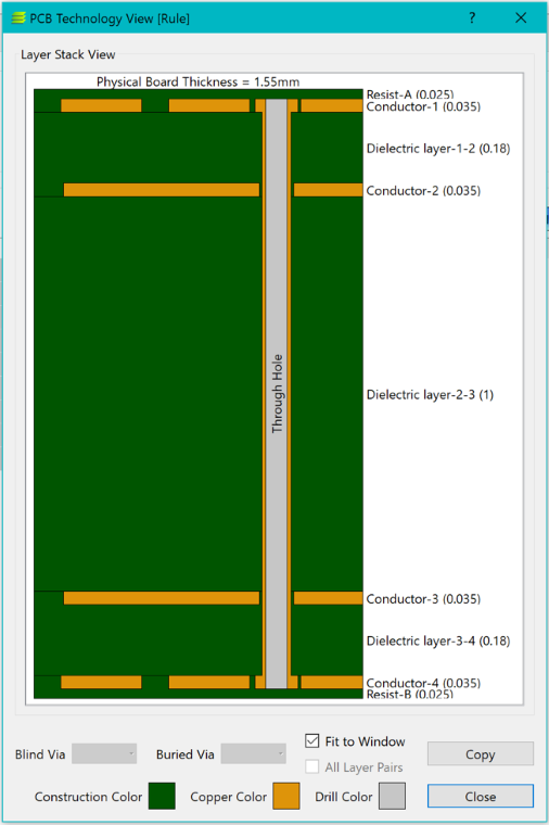
Figure 2: The PCB Technology View Dialog
This concludes the eCADSTAR Library Editor training. Close all open dialogs and exit eCADSTAR Library Editor.
Summary
During this course you have learned the basic functions of the Technology Editor and the Design Rule Editor. You can now create a new technology and design rule. For further information on eCADSTAR, and to continue your learning, you should now follow the eCADSTAR Schematic Editor training course.
