
Swapping Pins
In this topic, you will learn how to swap pins. This process allows you to optimize a layout, and is similar to swapping gates. Pin Swapping involves changing over the pin numbers of an Integrated Circuit (IC). For example, in the following NAND gate Integrated Circuit (IC) that you created, pins 1 and 2 could be swapped to aid routing, without any electrical effect on the circuit. This is demonstrated below.
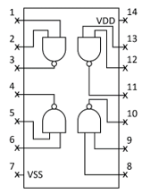
Figure 1: IC Containing Pins that can be Swapped
Specifying Pins that can be Swapped
The option to swap the pins in a part is configured in the library. This makes the option available to the layout engineer.
- In eCADSTAR Library Editor, open the part DIY-CD4093BM96.
- In Part Editor, select the Gate+Pin Equivalents tab.
- In the Gate+Pin Equivalents tab in Part Editor, select Symbol Pin 1 and Symbol Pin 2 of Gate:1-4 (DIY-NAND).
- Right-click the selected pins, and click Equivalent on the assist menu. The selected pins are shown as equivalent in the Gate+Pin Equivalents tab. This is illustrated in figure 2, below.
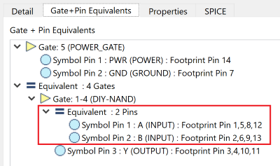
Figure 2 : Equivalent Pins
Swapping Pins
The following image shows the above NAND gate Integrated Circuit (IC) in eCADSTAR PCB Editor.
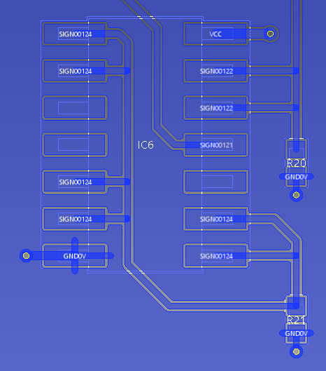
Figure 3: NAND gate Integrated Circuit (IC)
- To swap pins in eCADSTAR PCB Editor, select Net /Route > Net > Swap Pins on the eCADSTAR PCB Editor ribbon.
- Because Symbol Pin 1 and Symbol Pin 2 have previously
been specified as equivalent in eCADSTAR Library Editor,
selecting a padstack on this component highlights any footprint pins
with which the selected pin can be swapped. This is denoted by the
 (flag) icon, shown in figure 4, below. Because
footprint pin 1 is selected on the canvas, footprint pin 2 is identified
as a candidate for pin swapping. These footprints pins are shown in
Figure 2 as candidates for pin swapping.
(flag) icon, shown in figure 4, below. Because
footprint pin 1 is selected on the canvas, footprint pin 2 is identified
as a candidate for pin swapping. These footprints pins are shown in
Figure 2 as candidates for pin swapping.
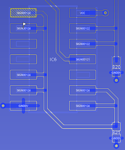
Figure 4: Pins Highlighted for Pin Swapping
- If you click , then the selected
footprint pins are swapped, and a confirmation dialog is displayed.
