Swapping Gates
As you build a part, you must map the symbol to the footprint. This involves defining which connections on the symbol connect to which pads on the footprint. In the case of a 14 pin Integrated Circuit (IC), for example, this task could be relatively simple. However, if you are building a more complex device such as a large FPGA, the task of mapping it could be more significant, although the mapping process is the same for both devices.
When a device contains multiple gates, such as the NAND Integrated Circuit (IC), you can swap gates during the layout stage of a design. For example, in the following illustration, each of the four gates performs the same function, and can be swapped without affecting the operation of the circuit. The schematic may have been drawn in a way that does not provide the optimal routing solution. If necessary, the engineer laying out the PCB can swap the gates to create the best routing solution. This topic demonstrates how to swap the gates on the following NAND gate Integrated Circuit (IC) that you created.
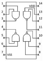
Figure 1: IC Containing Multiple Gates
Specifying Gates that can be Swapped
The option to swap the gates in a part is configured in the library. This makes the option available to the layout engineer. Equivalent gates are configured in the Detail tab in Part Editor. The symbol that is used for equivalent gates is specified in the Symbols section, in this tab. The mapping of footprint pins to symbol pins is defined in the Pin Assignment section.
- In eCADSTAR Library Editor, edit the part DIY-CD4093BM96.
- In Part Editor, select the Gate+Pin Equivalents tab, as shown below.
- Notice that information about each swappable gate is displayed here. The four gates all perform the same function, and can therefore be swapped without affecting the operation of the circuit. This will default to equivalents gates.
- To ensure no gate swapping can be performed each gate will require a unique name. For example, NAND2(1), NAND2(2), NAND2(3) and NAND2(4)
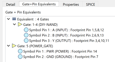
Figure 2 : The Gate+Pin Equivalents Tab
Swapping Gates
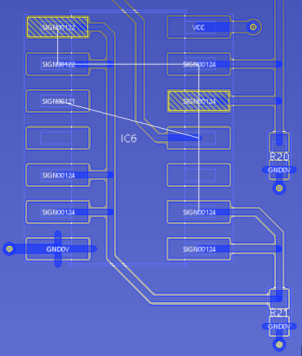
The following image shows the above NAND gate Integrated Circuit (IC) in eCADSTAR PCB Editor.
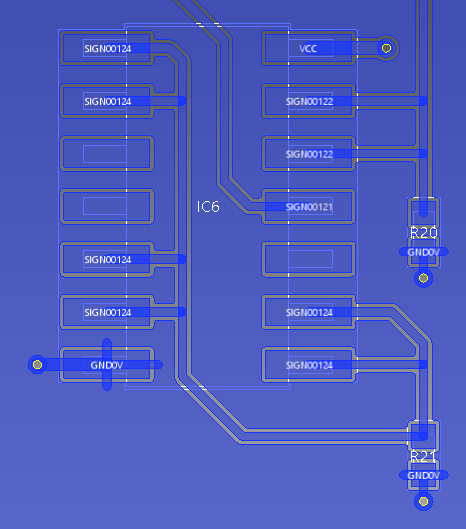
Figure 3: NAND gate Integrated Circuit (IC)
- To swap gates in eCADSTAR PCB Editor, select Net /Route > Net > Swap Gates on the eCADSTAR PCB Editor ribbon.
- Because gates have previously been specified as
equivalent in eCADSTAR Library Editor,
selecting a padstack on this component highlights the pins on gates
which can be selected for swapping. For Gates 1-4, shown in Figure
2, the footprint pins that are associated with symbol pins 1, 2 and
3 can be selected for swapping to another gate. This is illustrated
in figure 4, below, using the
 (ball) and
  (flag) icons.
- The (ball)
icon denotes a footprint pin that is associated with a gate that can
be swapped.
- The (flag)
icon denotes the possible footprint pins that can be selected when
swapping gates.
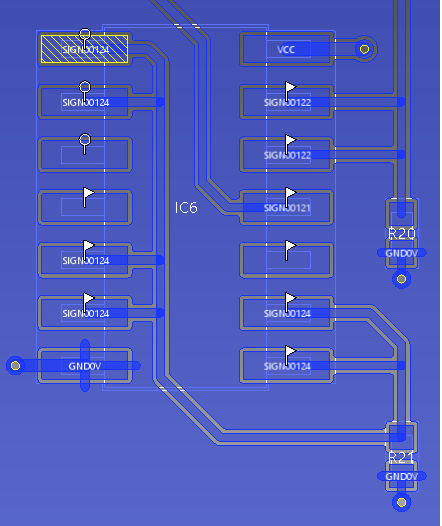
Figure 4: Pins Highlighted for Gate Swapping
- If you click on the highlighted
padstack on the right, then the gates that are associated with the
selected footprint pins are swapped. This is illustrated in the following
image.