
Setting the Supply and Consumption Source
This topic explains how to specify a component as a supply source in a Power Bus. It also describes how to specify the consumption power of components that are set as consumption sources.
- In the eCADSTAR PI/EMI Analysis module, select Tools > Check Supply Pin Definition on the menu. The Supply Pin Type Report dialog is displayed.
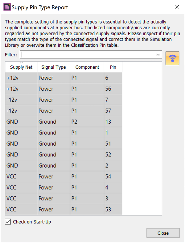
This dialog reports on component pins that are connected to power and ground pins but do not have a matching pin type assigned.
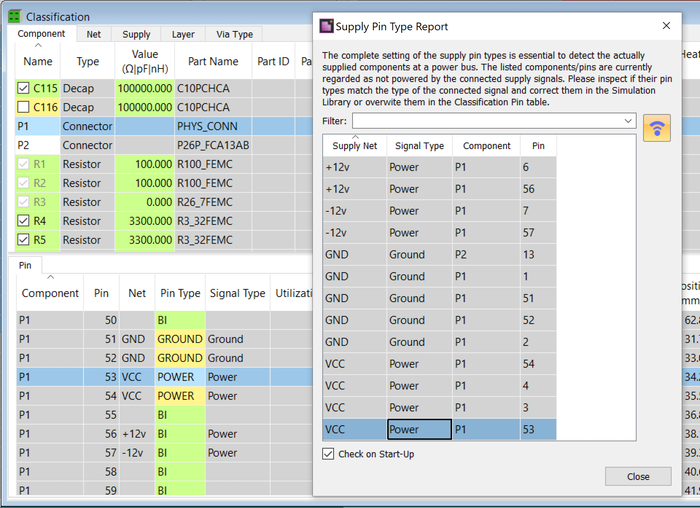
- Select a row in the grid for net GND connected to component P1. This will crossprobe to the relevant component and pins within the Classification view.
- For the highlighted pin in the Classification view, change the pin type to match the net name of the attached signal. For GND set to GROUND, and for VCC set to POWER. Repeat these steps for all GND and VCC items that are connected to component P1.
- Close and then reopen the Supply Pin Type Report dialog from the menu. The dialog no longer lists GND or VCC signals connected to P1. Close the dialog.
- Click the
 Classify
icon on the toolbar.
Classify
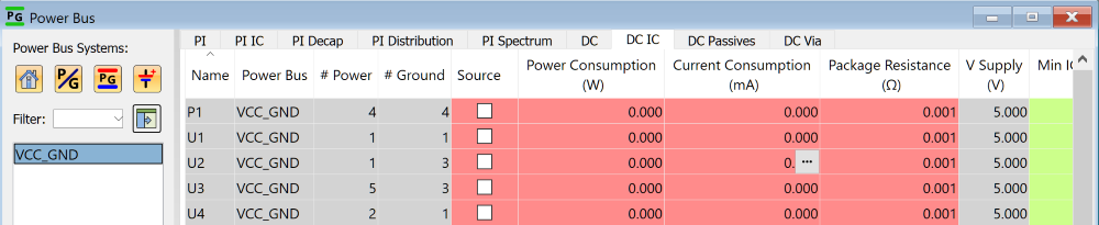
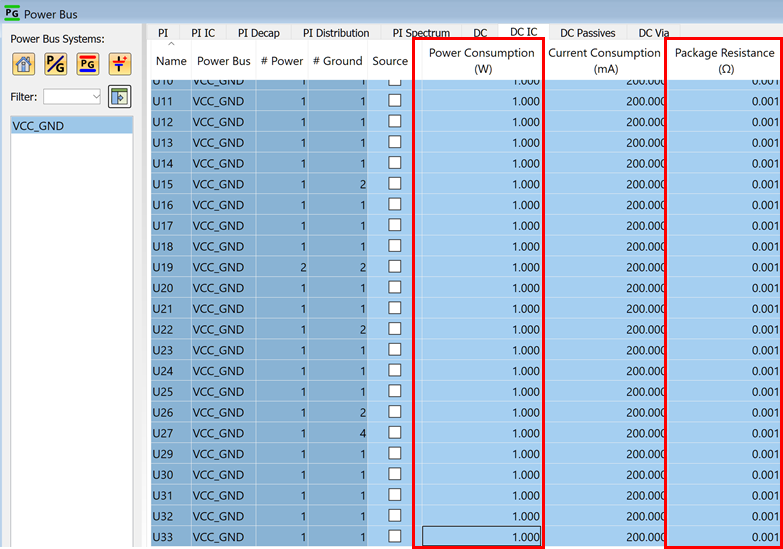
icon on the toolbar. - In the eCADSTAR PI/EMI Analysis module, Power Bus view, select the DC IC tab.
- In the Filter list, select VCC_GND. ICs that connect to the selected Power Bus are displayed.
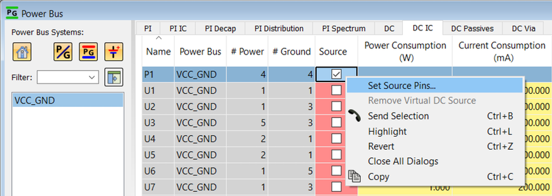
- To specify a supply source, select the Source check box for P1.
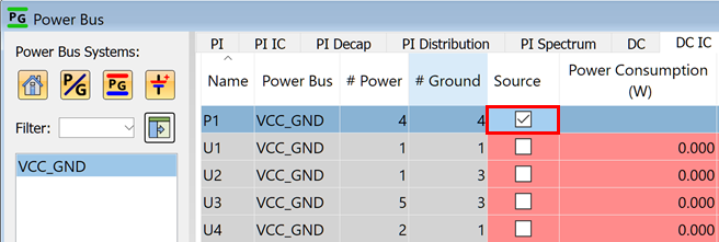
- To set the power consumption for each device, select all devices other than P1 using the Shift key and enter "1" in the Power Consumption column.
- In the Package Resistance column, use the default value of 1 mOhm.
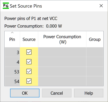
The supply source and consumption source can be specified for each pin. Right-click in the Source cell, and select Set Source Pins on the assist menu. Alternatively, click the
This task is demonstrated in the following video.
