
Introduction to the Technology and Rule Libraries
Technologies and rules are the foundations of eCADSTAR. They control the physical and electrical rules for your Printed Circuit Board (PCB) design. In this topic we will introduce you to both types of library.
The Technology Library
- The technology library is a single file which holds the layer definitions that are required to design printed circuit boards.
- Many different layer counts and configurations (technologies) can be contained in a technology library.
- A Technology itself only contains the layer types required for PCB design. It does not contain physical characteristics, material types or any manufacturing requirements.
- Each eCADSTAR PCB Editor design uses a technology that is selected from the library.
A typical layer definition is shown below.
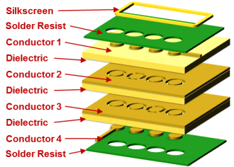
Figure 1: The Layer Stack
The Technology Library holds detailed definitions of PCB layer structures called “technologies”.
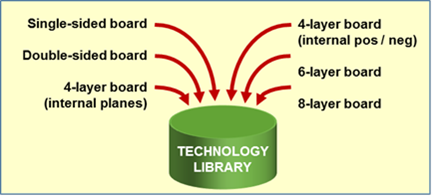
Figure 2: The Technology Library
Each technology contains the following elements:
- Technology Name: the user-defined name for a given technology.
- Number of Layers: this is automatically updated when electrical items are added or deleted.
- Layer Configuration: all layers that are required for PCB design (electrical, non-electrical and user defined). The layers are recognized by a “Layer Type”.
- Layer Mapping: this creates relationships between layer names in the footprint library and layer names in the PCB design.
- Layer Display Order: this defines the relative positions of the layers in the Layer View of the PCB design.
Layer Types
The following six layer types are available in technologies:
- System (Board Layers): non-conductive layers for board outlines, layout area, holes and slots and rule areas.
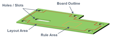
Figure 3: System layer usage
- Conductor: electrically conductive layers.
- Dielectric: isolating substrate material layers.
- System (Conductor Layer Related): non-conductive layers for symbol mark, solder resist and solder paste (metal mask). Each is associated with a conductor layer.
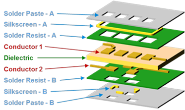
Figure 4: Layer build
- (Keepout/Other): component, track and via keepout layers associated with a conductor layer.
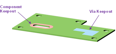
Figure 5: (Keepout/Other) layer usage
- User Defined:area fill (copper pour) template, documentation or manufacturing layers. These can be associated with conductor layers, as appropriate.
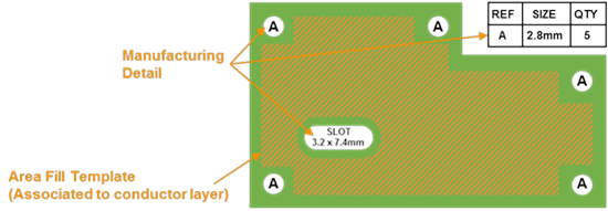
Figure 6: User defined layer usage
The Design Rule Library
- A design rule library is a single file which defines the general rules and constraints for all PCB designs.
- Board configuration rules are contained within the library. These rules define the exact layer stack-up parameters such as layer thicknesses, material types, dielectric constants and layer types. These are used to specify manufacturing requirements, and set the system parameters required to calculate impedances.
- Each design rule set references the technology library for the generic layer structures, which then have specification parameters added.
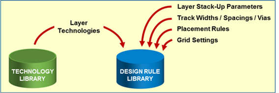
Figure 7: The Design Rule & Technology Libraries
You will complete the process of creating a set of design rules in Task 5.
