
eCADSTAR PCB Editor Introduction
Welcome to the eCADSTAR PCB Design training guide. This training guide will help you to understand the basic operations of eCADSTAR PCB Editor. You will be guided through the complete design of a sample PCB, from initial PCB creation to final manufacturing data output. This guide can be completed on its own, or as part of the full suite of eCADSTAR Training guides. A knowledge of the fundamental principles of designing printed circuit boards (PCBs) is required.
Tasks are provided that guide you through the design process. You can complete each task, or simply open the supplied designs at each step to continue at your own convenience.
eCADSTAR Architecture
The diagram below shows the complete Library system and interactions with other eCADSTAR tools.
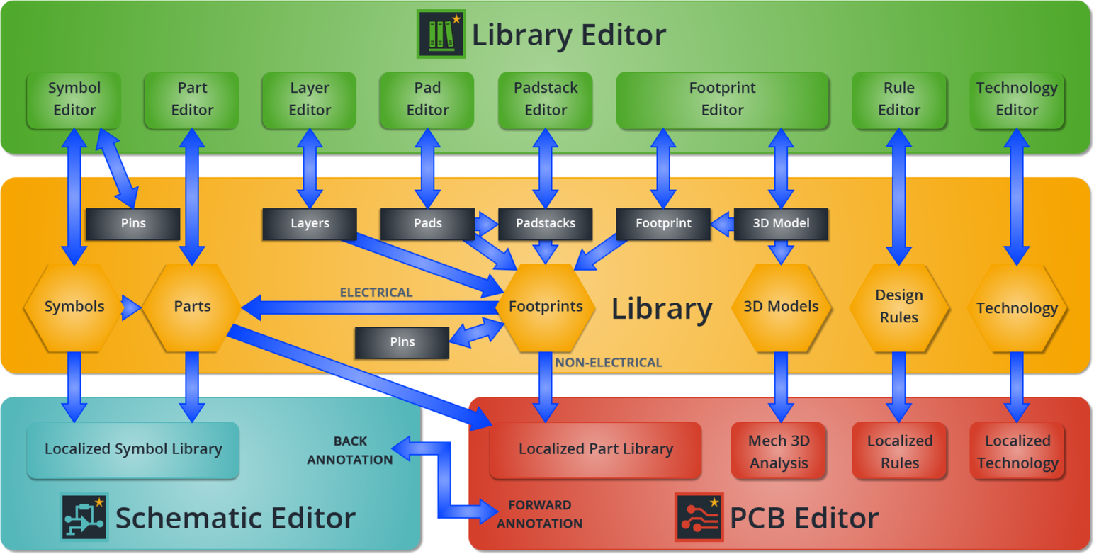
Figure 1: The Complete eCADSTAR System
eCADSTAR Library Editor can be opened from within the eCADSTAR PCB Editor. The Component tab has a on the ribbon:
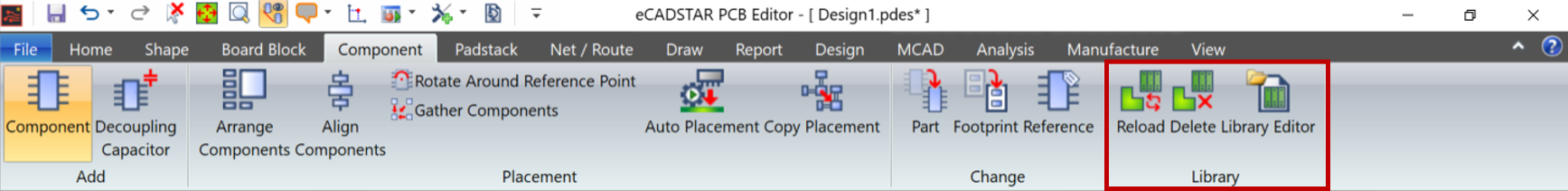
Figure 2: Accessing Library Editor in PCB Editor
Library’s interaction with PCB Editor
When you create a schematic or PCB design, Schematic and PCB Editors reference the same library. You can also edit PCB technologies and design rules in eCADSTAR PCB Editor.
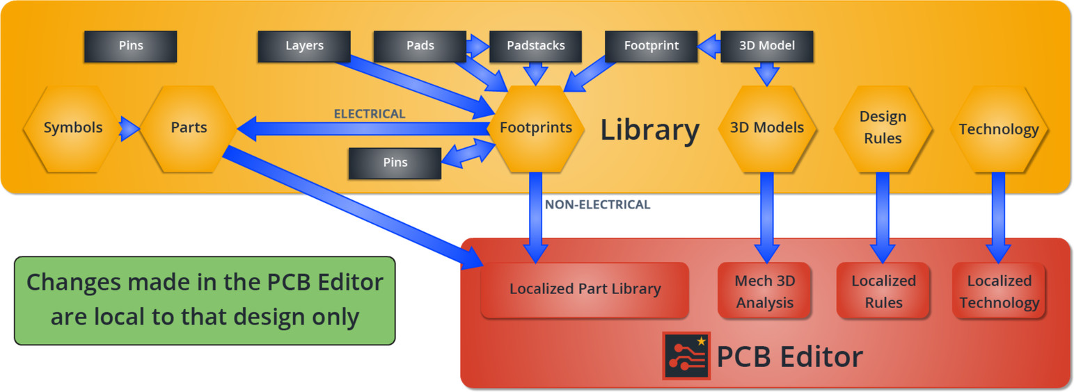
Figure 3: The Library's interaction with eCADSTAR PCB Editor
The localized library in eCADSTAR PCB Editor contains parts, rules, technologies, pads, padstacks and footprints. The localized library in eCADSTAR Schematic Editor contains parts and symbols.
Training Files
Data is provided to enable running this training without completing the other aspects of DIY training.
- Library [Default installation folder]: this defines the Technology (PCB Layer Mapping), Design Rules (PCB Spacing Rules), parts, footprints, padstacks and pads.
- Schematic [Default installation folder]: this contains the components and connectivity for the PCB.
-
PCB files that are provided, and their current state:
- Design1.pdes: Board Outline.
- Design2.pdes: Modified board outline. Layout area added.
- Design3.pdes: Modified board outline. Layout area and holes added.
- Design4.pdes: Components placed and aligned. Fiducials added.
- Design5.pdes: Routed, but not flooded.
- Design6.pdes: Templates and planes added.
- Design7.pdes: Silkscreen completed.
- Design8.pdes: Complete.
- Design9.pdes: DRC Errors included.
This guide will cover the following topics:
- eCADSTAR PCB Editor Interface
- PCB Generation
- Component Placement
- PCB Routing
- Post Design Checking
- PCB Cosmetics
- Manufacturing Outputs
Upon completion of this training, you will have a basic understanding of the capabilities of eCADSTAR PCB.
Launching eCADSTAR PCB Editor
- Select eCADSTAR PCB Editor from the Start button.
- Select Open > Design from the File menu.
- Open the design “C:\Users\Public\eCADSTAR\eCADSTAR [version]\Designs\DIY_Training\PCB\Design8.pdes”
