
Task 6: Grouping Components for Placement, and Specifying a Track Width Stack
You can group components in eCADSTAR Schematic Editor to enable them to be easily placed together in eCADSTAR PCB Editor. The procedure shown below describes how to group the FLASH memory with its connected resistors and capacitor.
- If you completed your own version of the entire DIY training schematic design, as described in the note at the bottom of Task 5, then continue to use that design.
- If you did not complete your own version of the design, then continue to follow the DIY Training using this sample DIY training schematic design: C:\Users\Public\eCADSTAR\eCADSTAR [version]\Designs\DIY_Training\SCH\DIY_Training\DIY_Training.sdes.
- In eCADSTAR Schematic Editor, select the five components shown below by clicking the first item, and then pressing Ctrl and clicking other items.
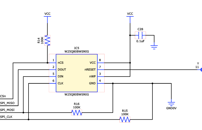
Figure 1: Selecting Components
- On the eCADSTAR Schematic Editor ribbon, display the Properties panel by clicking View > Display > Properties.
- In the Properties panel, specify "NFLASHCOMPS" in the Placement Group row. This setting will gather the selected components for placement in eCADSTAR PCB Editor. However, because the decoupling capacitor pin must be very close to the VCC pin on the memory device, another setting is required, which is described below.
- On the status bar, change the selection filter so that component pins will be selected, as shown below.
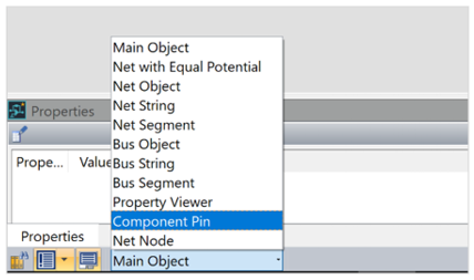
Figure 2: Setting the Selection Filter
- On the eCADSTAR Schematic Editor ribbon, click Design > Snap > Snap split button > Snap Settings. The Snap Settings dialog is displayed.
- In the Snap Settings dialog select Only allow snap point selection, as shown below.
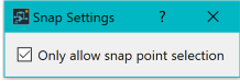
Figure 3: Snap Settings
- Close the Snap Settings dialog.
- On the eCADSTAR Schematic Editor ribbon, click Design > Snap > Snap to toggle on snapping.
- On the schematic, click the VCC pin on IC5 to select it.
- Press Ctrl on the keyboard, and click the connected pin on C28 to select it.
A flag is displayed as you point the cursor at each pin location. This turns to a cross after you click.
Figure 4: Pins Selected
-
In the Properties panel, specify "NFLASHDECAP" in the Placement Group row. When IC5 and C28 are gathered for placement in eCADSTAR PCB Editor, the power pin of IC5 will be close to the capacitor pin. After placement and routing, this part of the completed design appears as shown below.
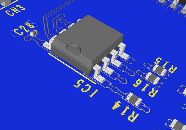
Figure 5: NAND Flash and Associated Passive Components after Placement and Routing
- Assign a Track Width Stack value to the PS2_ENSS_REG net as follows: on the eCADSTAR Schematic Editor ribbon, select Home > Find > Find. The Find dialog is displayed.
- In the Find dialog, specify the following values and click Find All.
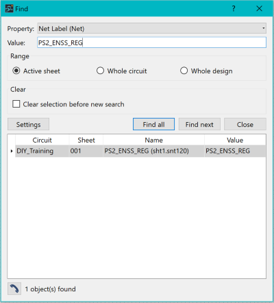
Figure 6: The Find Dialog
- In the Find dialog, results table, double-click the PS2_ENSS_REG net. This net is highlighted on the canvas, and displayed in the Properties panel.
- In the Properties panel, specify a value of 0.2mm in the Track Width Stack row.
Track width stacks can provide detailed information on the track widths for each layer, and extra settings such as routing direction. You can set a track width stack for one or more nets that you select in eCADSTAR Schematic Editor. For example, you might select nets for which the correct widths for impedance control on each layer are required.
Track width stacks are created in the Rule Editor dialog, Tracks tab in eCADSTAR PCB Editor. In the following example, the track width stacks "0.1mm”, “0.2mm”, “0.4mm”, “0.6mm” and “50R” have been created in the Track Width Stack section. To specify one of these values in eCADSTAR Schematic Editor, you must enter the required name in the Properties panel, Track Width Stack row.
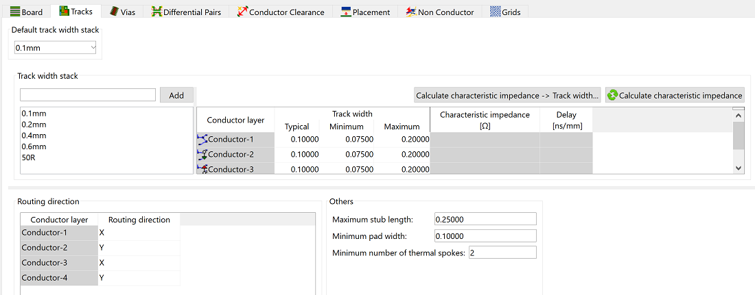
Figure 7: The Rule Editor dialog
This task is demonstrated in the following video.
