
Task 28: Analyzing the Design and Correcting Issues
In this task, you will analyze the design with the Routing Consultant, and correct the issues that are found.
- Load the design unrouted.pdes into eCADSTAR PCB Editor.
- On the canvas, select the routing area routing_area1.
- Select Net / Route > Autorouting > Autorouter on the eCADSTAR PCB Editor ribbon. The Routing Strategy dialog is displayed.
- In the Routing Strategy dialog, clear the existing strategy by clicking New.
- Click Consultant to launch the Routing Consultant dialog. The Consultant Options dialog is also displayed.
- In the Consultant Options dialog, Analysis Level section, select High and click OK. This is illustrated below.
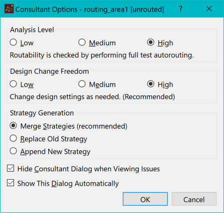
Figure 1: The Consultant Options Dialog
- In the Routing Consultant dialog, click Analyze. The consultant will analyze the design. Results are displayed in the Routing Consultant dialog.
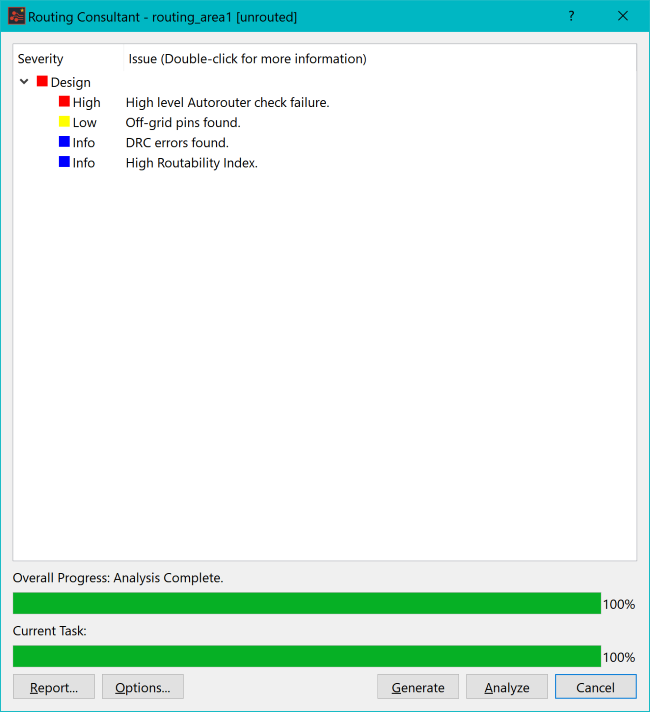
Figure 2: Analysis Results
- Double-click the first item in the list. This is the high-severity item, "High Level Autorouter check failure". An explanation is provided in the displayed Issue Description dialog.
- In the Issue Description dialog, click the GND0V hyperlink, as illustrated below.
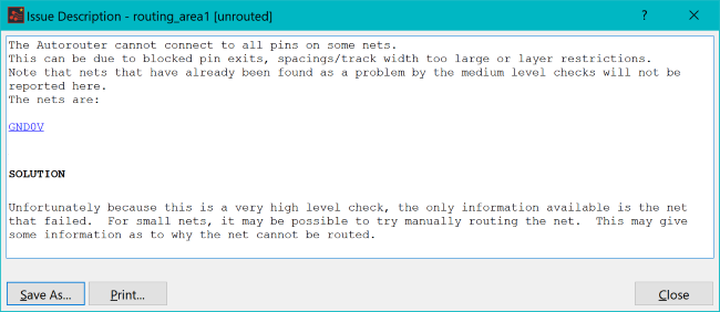
Figure 3: Potential Pin error
-
Confirm that the item is selected on the canvas in eCADSTAR PCB Editor, as shown below. Note that the complete GND0V net is highlighted.
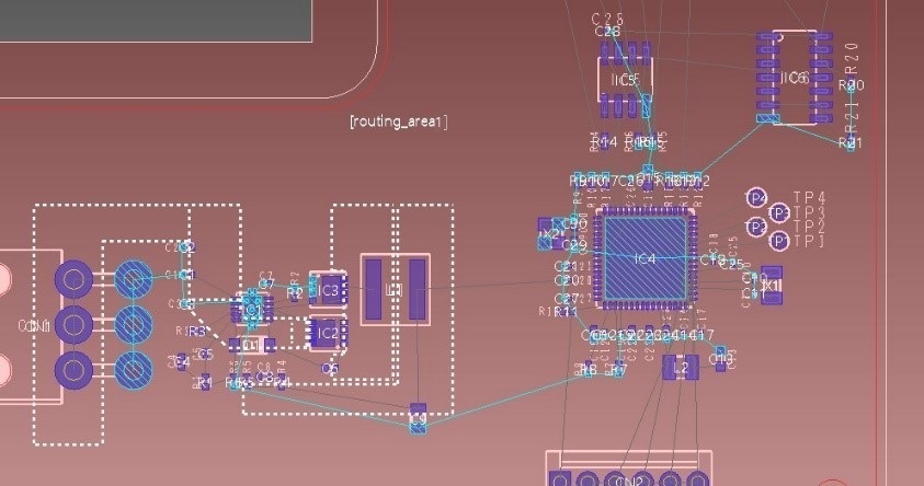
Figure 4: Cross Probing from the Issue Description Dialog
The error listed by the routing consultant is shown as a “Autorouter check failure” because the Autorouter is unable to connect all GND0V nets together. This was highlighted in Task 27 for the Ground pad on IC4.
This procedure is demonstrated in the following video.
