
Defining the Layer Configuration
Defining the Material Characteristics.
- If not already running, click eCADSTAR [Version] > PCB Editor [Version] on the Start menu to launch eCADSTAR PCB Editor.
- On the File tab, click Open. Alternatively, click Open on the Home tab. The Open dialog is displayed.
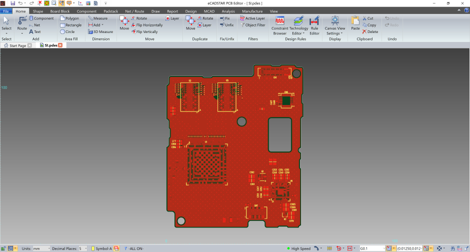
- Browse to the following location and click Open: C:\Users\Public\eCADSTAR\eCADSTAR [Version]\Analysis\SI_PCB\SI.pdes.
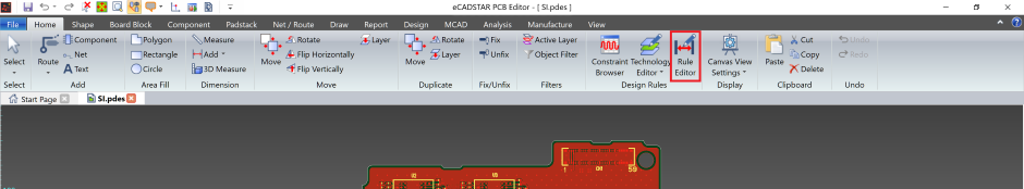
- On the ribbon, click Home > Design Rules > Rule Editor. Rule Editor dialog is displayed.
- Select the Board tab, and check the layer definitions are as shown below.
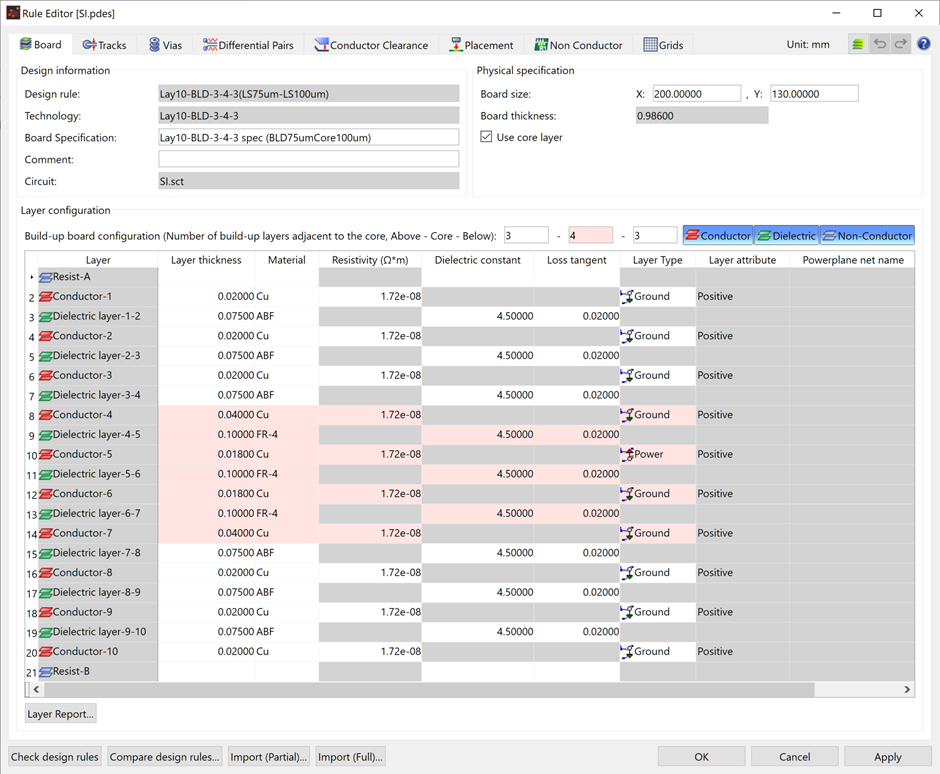
Reference Planes
A field solver requires a layer that is identified as a reference plane. A layer with the Layer Attribute set to Power-plane is always handled as a reference plane. However, it is possible to have a positive or positive/negative layer identified as a reference plane by defining their electric layer type. If there is no power plane, you must define a reference plane for two or more layers.
- In Rule Editor, check the entries in the Layer attribute column on the Board tab. The design data does not contain a layer whose layer attribute is set to powerplane. However, as the electric layer type definition is set to power signal or ground signal, each layer is identified as a reference plane.
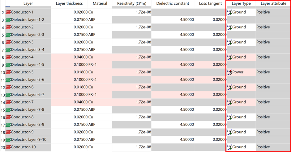
- The fact that the electric layer type definition
is set to power or ground does not mean that you cannot route general
signals.
- In electromagnetic analysis, a reference plane refers to a stable potential plane. Therefore, if a reference plane is defined for a routing layer with smaller area fills, then analytic errors become larger. Also, if Enable enhanced plane extraction is specified in the topology extraction options, then the true shape of a power or GND net is considered.
Defining a Resist Layer
A resist layer must be defined to perform more precise simulation. Taking a solder resist into account allows you to consider detailed cross-section models.
- Enter the following values for the Resist-A
and Resist-B layers.
Layer thickness: 0.02
Material: mat1
Dielectric constant: 4.5
Loss tangent: 0.02 - Click OK. A confirmation
dialog is displayed, as shown below.
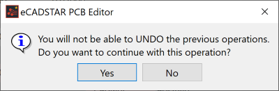
- Click Yes to close the Rule Editor.
This task is demonstrated in the following video.
