
Task 13: Creating Templates on Outer Layers
In this section you will complete the outer layers of the routed PCB by adding more templates. Continue to use the design that you created in Task 12 for the following task. You will create multiple templates on the top layer.
If you did not complete steps 4-8 in the preceding task, then you must complete steps 1-5 below. If you completed all steps in the preceding task, then ignore steps 1-5 below.
- In the Net/Route tab, click Template Area Settings. The Template Area Settings dialog is displayed. In this dialog you will associate the conductor layers with template layers. This step can be skipped if using supplied design Design5.pdes. This is an optional step. See the Note above.
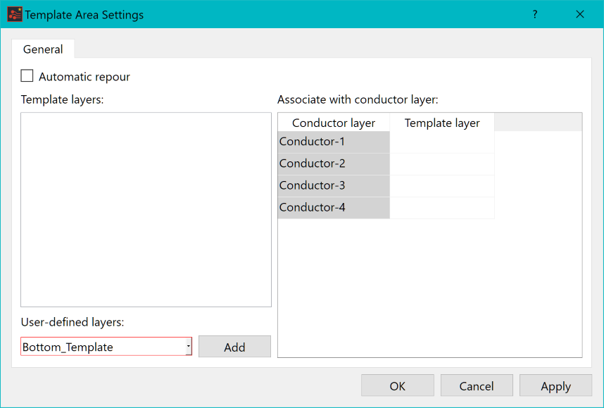
Figure 1: Template Area Settings Dialog
- In the Template Area Settings dialog, ensure that Automatic repour is selected. This is an optional step. See the Note above.
- From the User-defined layers pull down list, select Inner_Signal2_Template and click Add. Repeat for the Inner_Signal3_Template, Top_Template and Bottom_Template layers. This makes these layers eligible for template use. This is an optional step. See the Note above.
- In the Associate with conductor layer dialog, for each of the cells in the Template layer column set:
- Top_Template for Conductor-1
- Inner_Signal2_Template for Conductor-2
- Inner_Signal3_Template for Conductor-3
- Bottom_Template for Conductor-4
This is an optional step. See the Note above.
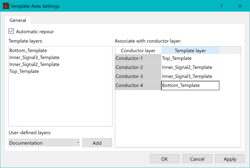
Figure 2: Template Area Settings Dialog (Configured)
- Click OK. This is an optional step. See the Note above.
- Ensure that Conductor-1 is displayed and Conductor-4 is not displayed in the Layer settings dialog.
- Set Conductor-1 as the Active layer.
- Set your window zoom to resemble the image shown below.
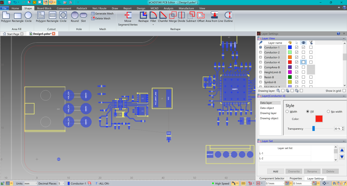
Figure 3: Setting the Zoom Window
Firstly, you will create additional templates on the top layer. These are shown below and are connected to the supplies:
- VIN_12V
- PS2_BOOT_REG
- VCC
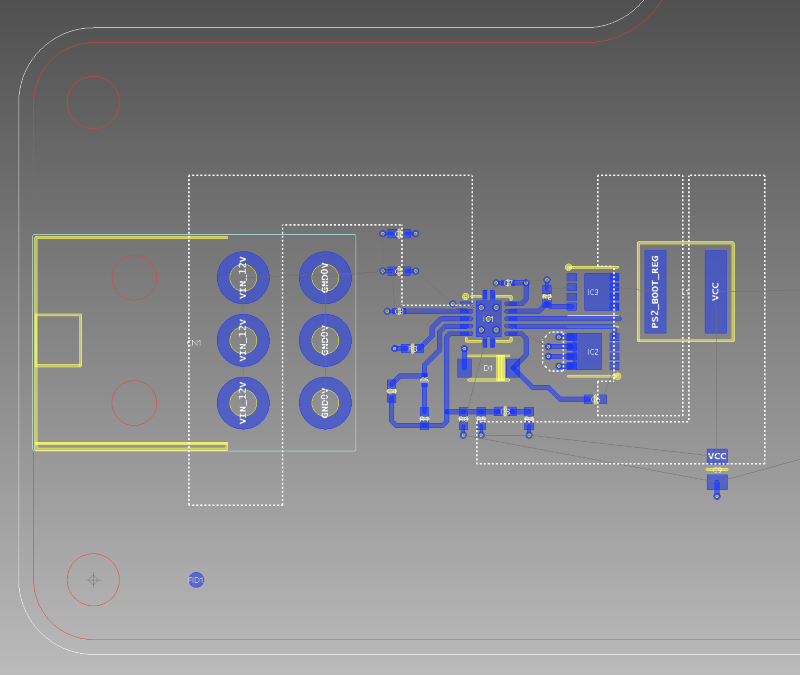
Figure 4: Creating Additional Templates
- On the eCADSTAR PCB Editor ribbon, select Shape > Area Fill > Polygon.
- In the Area Fill (Polygon) dialog, Thermal relief row, click Settings and set the values shown below.
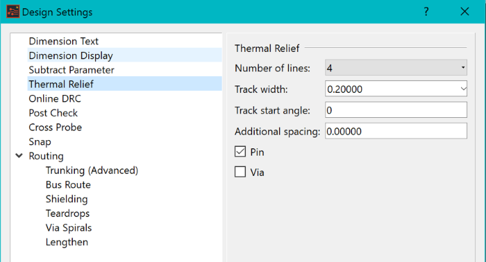
Figure 5: Setting Thermal Relief Values
- Click OK.
- In the Area Fill (Polygon) dialog, Subtract parameter row, click Settings and ensure that the Allow isolated figure check box is not selected.
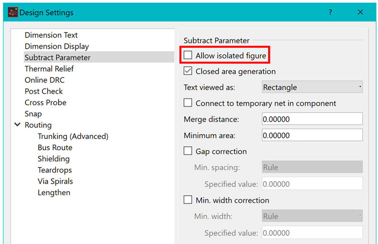
Figure 6: Checking the Isolation Generation Box
- Click OK.
- From the Area Fill (Polygon) dialog set Template area to ON.
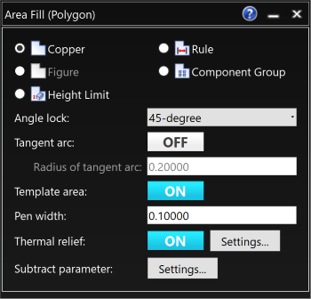
Figure 7: Setting the Template Area
- Locate the supply VIN_12V by pointing the cursor at the PCB, and clicking the mouse to attach it to the cursor.
- Click the start point of the template and replicate it as shown below.
- Right-click and select Finish when complete.
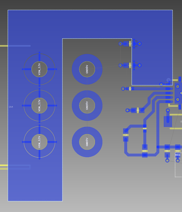
Figure 8: Adding a Template Area
- Repeat the above operation to create templates PS2_SW_REG and VCC as shown below.
- Add an extra VIN_12V area definition next to IC2
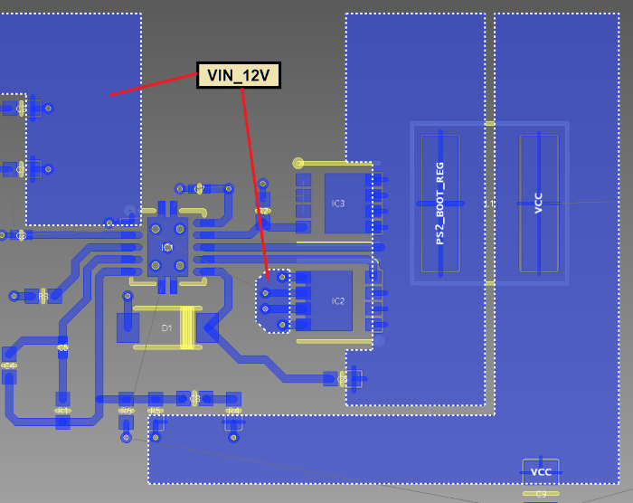
Figure 9: Creating Additional Template Areas
Now, define a GND0V template for the outer layer:
- On the eCADSTAR PCB Editor ribbon, select Shape > Area Fill > Rectangle.
- Locate GND0V by pointing the cursor at the PCB and clicking the mouse to attach it to the cursor.
- Click outside the bottom-left edge of the board, and drag the cursor across the board. Click again when outside the top-right edge. The template copper is poured as shown below.
Figure 10: Creating a Copper Flood Area
- Repeat the above exercise to add a template on Conductor-4 for the net GND0V.
This task is demonstrated in the following video.
