
Verifying I/O Common Mode Noise
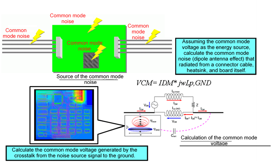
The common mode noise verification in eCADSTAR verifies phenomena where a connector cable, board or heatsink turns into a dipole antenna, and generates a noise.
This function analyzes the voltage fluctuation of a reference plane that is generated by the impact of crosstalk interference from general signals. Then it calculates the EMI noise, in which the reference plane itself is assumed to be the energy source. A connector cable, board or heatsink is assumed to be an arm of a dipole antenna.
The following procedure describes how to display the analysis result, and visualize the impact on the reference plane in a color map, by listing the impact levels. This allows you to identify the signal (true noise source) that affects the reference plane.
- In the PI/EMI Analysis module, select the Radiation view.
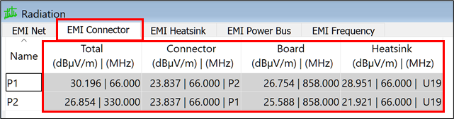
- Select the EMI Connector tab. This shows the result of analysis where a cable is assumed to be dipole antenna arms (single or both). For each connector, it represents the impact caused between other connectors, the board, or heatsinks.
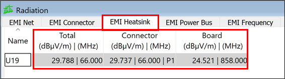
- Select the EMI Heatsink tab. This shows the result of analysis where a heatsink (IC) is assumed to be a dipole antenna arm (single). For each heatsink, it represents the impact caused between connectors or the board.
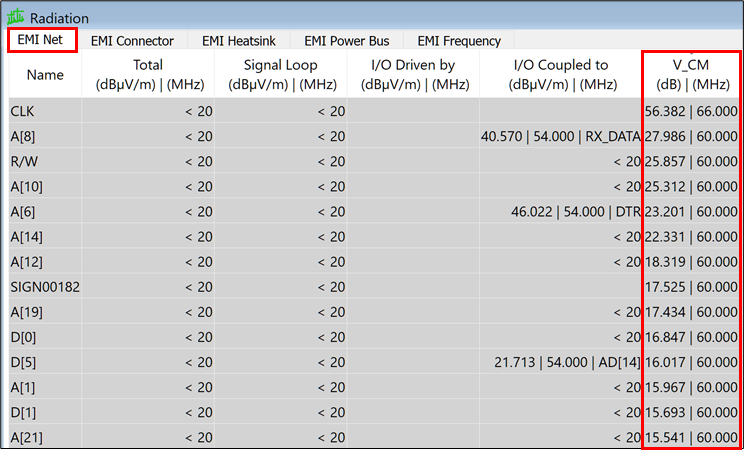
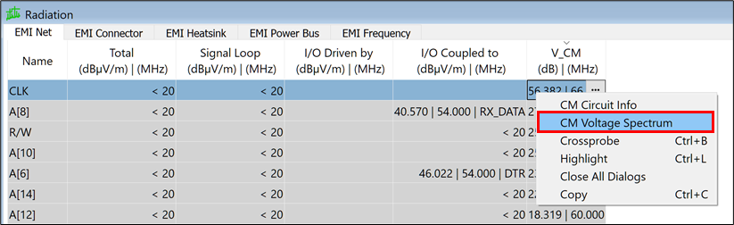
- Select the EMI Net tab, and click the V_CM (common mode voltage) column label. This sorts the values in descending order. Note that the value of "CLK" is the largest. As the common mode voltage represents the degree of common mode voltage drop, this indicates that "CLK" is the primary cause of the common mode noise.
Common mode voltage drop represents a phenomenon and behavior where a reference plane changes in voltage. This change in voltage may be a current source, which is generating the common mode noise. The change may be caused by the impact on the reference plane of crosstalk interference from other signals. The analysis result indicates whether this problem has actually occurred.
- Right-click the cell in the V_CM column for the "CLK" net, and execute CM Voltage Spectrum.
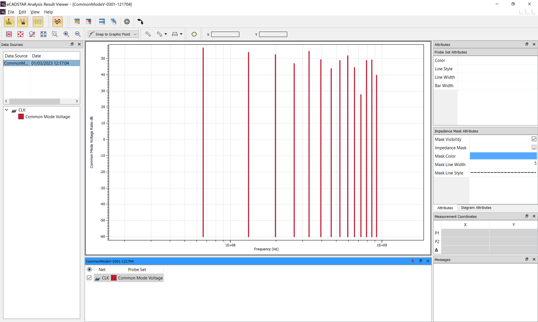
- The Analysis Results Viewer dialog is displayed. This shows the change in voltage of the reference plane that is caused by this CLK in frequency distribution.
- Select File > Exit to close the eCADSTAR Analysis Results Viewer dialog.
- On the eCADSTAR PCB Editor canvas, click an area outside of the board to clear the current selection.
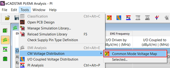
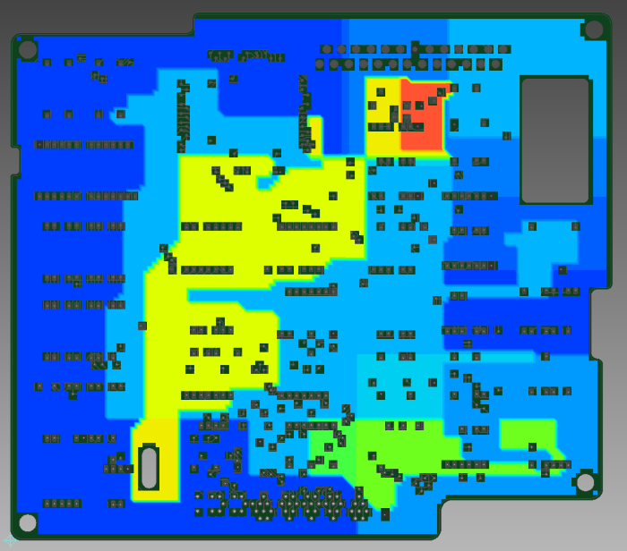
- To display a map for the board, related to the reference plane’s change in voltage: on the menu bar of the PI/EMI Analysis module, select Tools > CM Voltage Distribution > Common Mode Voltage Map.
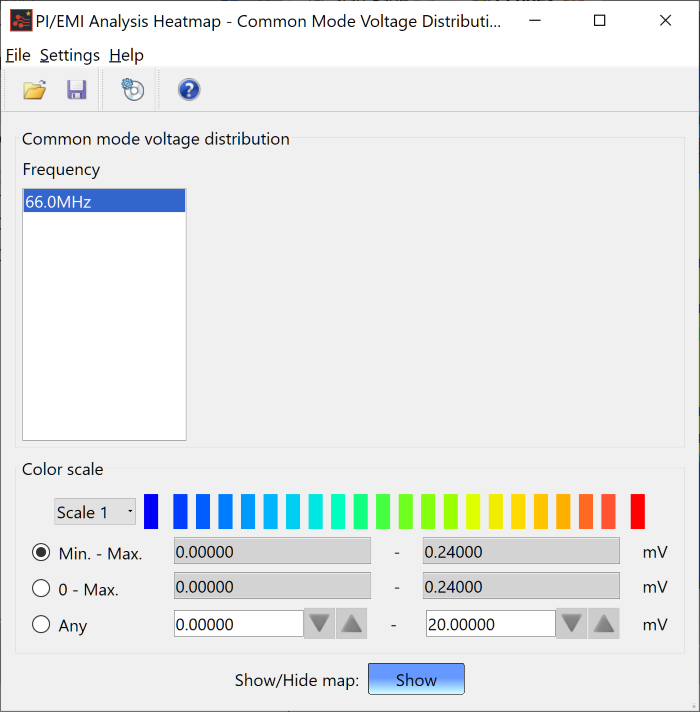
- The PI/EMI Analysis Heatmap dialog now shows the common mode voltage distribution. On the canvas, the voltage distribution for the worst case (peak frequency band) is displayed in a color map for the reference plane's change in voltage.
This task is demonstrated in the following video.
