
Task 6: Setting the Track Specification
In this task you will create a track width stack. The track width stack is used in the PCB design to define allowable track widths per layer. Note that several track widths can be defined.
- Click the Tracks tab, as shown in figure 2.
- In the Track width stack box, enter "0.1mm", and click Add.
- In the Default track width stack box enter "0.1mm", as shown below.
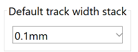
Figure 1: Setting the Default Track Width Stack
-
Set the Typical value to "0.10000 ", the Minimum value to "0.07500" and the Maximum value to "0.20000" in the Track width grid for all conductor layers, as shown below.
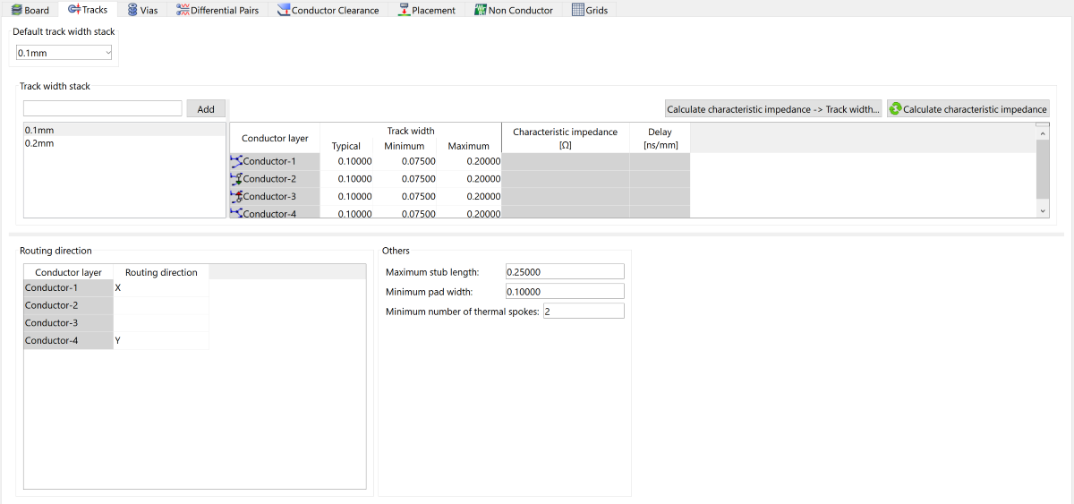
Figure 2: Track Width Settings
Note
When routing a board, the Typical track width is the value that is used by default.
When routing a board, the Typical track width is the value that is used by default.
- Follow steps 2 and 4 above to create another track width stack named "0.2mm", with “0.20000” typical, "0.15000" minimum and "0.50000" maximum.
- In the Routing direction section, Routing direction column, specify "X" for Conductor-1 and "Y" for Conductor-4.
- Remove the Routing direction values for Conductor-2 & Conductor-3. These are power and ground plane layers.
- In the Others section:
- Set the Maximum stub length value to "0.25000".
- Set the Minimum pad width value to "0.10000 ".
- Set the Minimum number of thermal spokes value to "2".
Note
The values that you enter in the Routing direction and Others sections apply to the entire board.
The values that you enter in the Routing direction and Others sections apply to the entire board.
- Click Save. Any
warnings that are displayed can be ignored at this stage. This task is
demonstrated in the following video.
You have now added the required track width stacks, with their minimum and maximum permitted values.
