
Task 7: Creating the Via Specification
In this task, you will create the specifications of the required via. You will define the padstacks that can be used for creating vias, and define the connected span in the board for those vias.
Defining the Padstacks
- Select the Vias tab.
- Enter "v45" in the Padstack Filter box, and then select v45h20m30 from the results, as shown below. Alternatively, scroll down the list and select v45h20m30 (via 0.45mm pad, 0.2mm hole, 0.3mm mask). The padstacks are read directly from the footprint library.
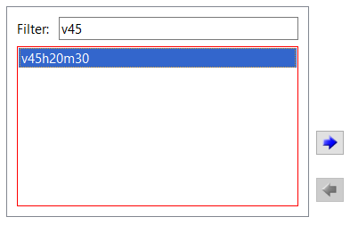
Figure 1: The Padstack Filter Box
- Click the
 button
to the right of this list to add it to the list of Available
padstacks.
button
to the right of this list to add it to the list of Available
padstacks. - In the Default padstack combo box, select v45h20m30 to make it the default.
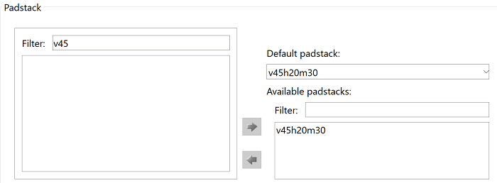
Figure 2: Setting the Default Padstack
- Repeat steps 2 and 3, above, for the padstack v80h50m60.
- On the ribbon, click File > Save. Ignore any errors or warnings that are displayed.
This procedure is demonstrated in the following video.
Setting the Via Span
Via spans can be set in the Via Layer Span section, for through-hole, blind, buried and build-up vias. They are used to define the layers which a via will connect. For example, whether the via will penetrate through the full depth of the board, or will only span certain layers. These layer spans are known as “from-to”.
- To define a through-hole via: click and drag from cell 1 down to cell 4. A via layer span is created.
- On the ribbon, click File > Save. Ignore any errors or warnings that are displayed.
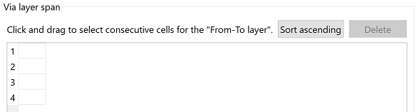
Figure 3: Via Layer Span Grid
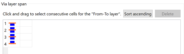
Figure 4 : Via Layer Span Grid with Layer Pair set
This procedure is demonstrated in the following video.
You have now created the via specifications required for this training. Note that the Via Layer Span section can also be used to define the connection spans for blind, buried and build-up vias. You can also assign a specific padstack to a defined via layer span (known as a “conditional padstack”).
Differential Pairs
This tab contains the options that allow you to create a differential pair rule stack. This is used in the board to control the PCB rules relating to differential pairs. However, these settings are not required in this design.
