
Task 12: Configuring Non Conductor Settings
In this task, you will use the Non Conductor tab to set symbol mark specifications, and allowable placement angles. This tab contains the allowable symbol mark rotation, and text sizes. The clearances for solder resist, and symbol mark to other features are also set here.
-
Click the Non Conductor tab, as shown below.

Figure 1: Non Conductor Settings
- Click in the Minimum text width box, and enter the value "1.50000".
- In the Minimum text height and Minimum text spacing boxes, enter the values "1.50000" and "0.15000" respectively. This will ensure that the text for the symbol mark layer is clear and readable on the manufactured board.
- Set the angle restrictions for text to be "0" and "90" on Side A and Side B by ticking the relevant boxes. This will ensure that the text, for the symbol mark layer, is clear and readable on the manufactured board.
- In the Clearance section, for Resist – Resist, set the values for Wave to be "0.15000" and Single Reflow/Reflow to be "0.25000".
- In the Clearance section, for Resist – Conductor, set the values for Wave to be "0.15000" and Single Reflow/Reflow to be "0.25000".
- Set the value for Symbol Mark – Hole and Symbol Mark – Resist to be "0.15000".
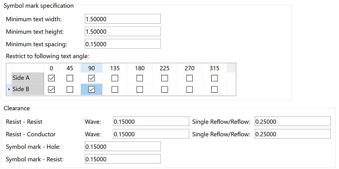
Figure 2: Symbol Mark Settings
- On the ribbon, click File
> Save. At this stage, ignore any warnings or errors.
This task is demonstrated in the following video.
