
Library Layers
Library layers are used to place individual items when building component footprints or padstacks. An example of library layers is shown below.
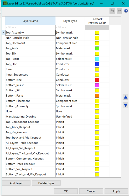
Figure 1: Library Layers
Layer Name
User definable layer name.
Layer Type
Defines the layer type of the library layer. This can be set to the following:
- Component Area: contains areas of components that are checked using the DRC command. The heights of components are also checked if a 3D model is not found.
- Conductor: used for conductors. Multiple conductor layers can be specified.
- Hole: used for holes. Only one Hole layer is permitted in a board design.
- Inhibit: used for keepout areas between tracks, between vias, and between tracks and vias.
- Metal Mask: used for metal mask (Solder Paste) data.
- Non-circular hole: used for cutouts. Only one Non-circular hole layer is permitted in a board design.
- Solder Resist: used for solder resist data.
- Symbol Mark: used for symbol mark (Silkscreen, Assembly outlines) data.
- User defined: additional layers that you define. These are commonly used for notes or dimension data. Multiple user-defined layers can be specified.
Padstack Preview Color
The preview color for padstacks can be specified for each layer. The preview color is displayed in the Padstack Editor preview.
Note
- As a minimum requirement in Footprint Editor, two component area layers and one hole layer are required.
- Library layers should be defined to suit both Surface Mount Technology (SMT) and Plated Through-Hole (PTH) components. An example is shown below.
- Keep the number of layers in the library to a minimum.
- Use "one-to-many" layer mapping whenever possible.
- As library layers do not relate directly to the PCB technology layers, mapping is required. The mapping is covered in the Technology and Design Rule Editors training.
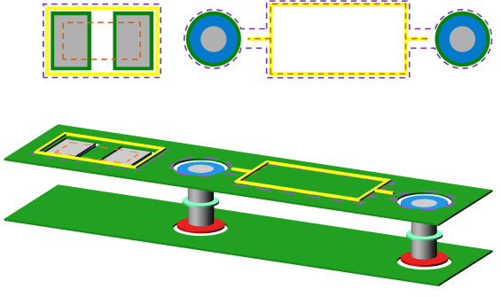
Figure 2: Example of Library Layers
