
Task 4: Checking Transmission Lines
This topic describes how to check transmission lines in eCADSTAR PCB Editor.
- On the Status Bar in eCADSTAR PCB Editor, click Coupling for Analysis to enable this command.
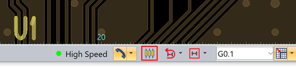
When performing SI analysis or viewing signal topologies, the Coupling for SI Analysis button allows you to specify whether coupling is considered.
 Deselected: coupling is not considered.
 Selected: coupling is considered.
Processes with coupling taken into account cannot be executed when multiple signals are selected.
- On the ribbon, click the Analysis > SI > Extract Scenario pull down arrow. From the pull-down menu, select Extraction Options.
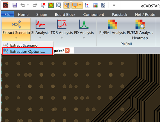
The Extraction Options dialog is displayed.
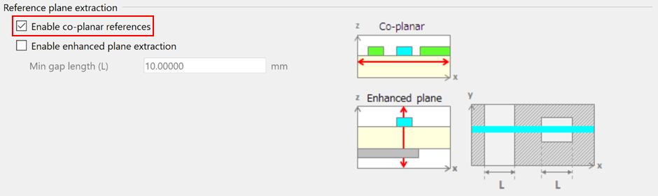
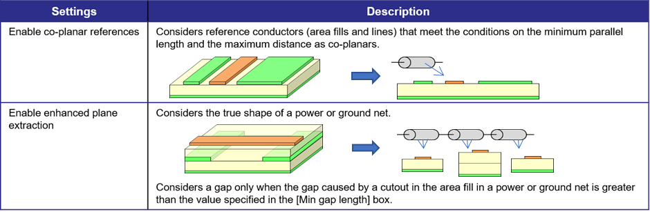
- Select Enable co-planar references in the Reference plane extraction section.
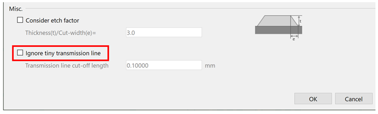
- Deselect Ignore tiny transmission line in the Misc section, and click OK to close the dialog.
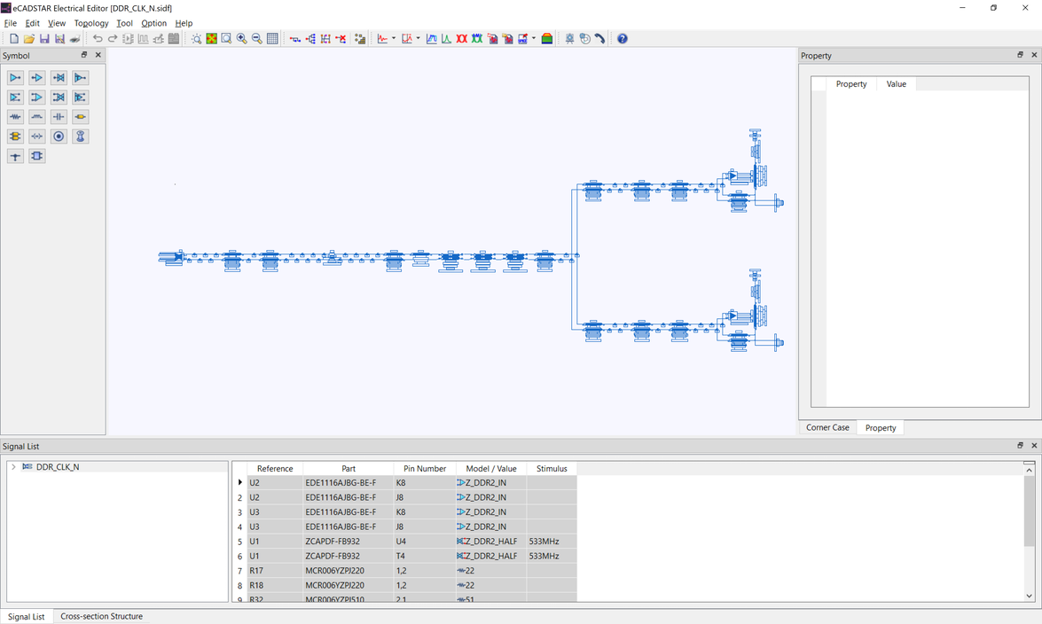
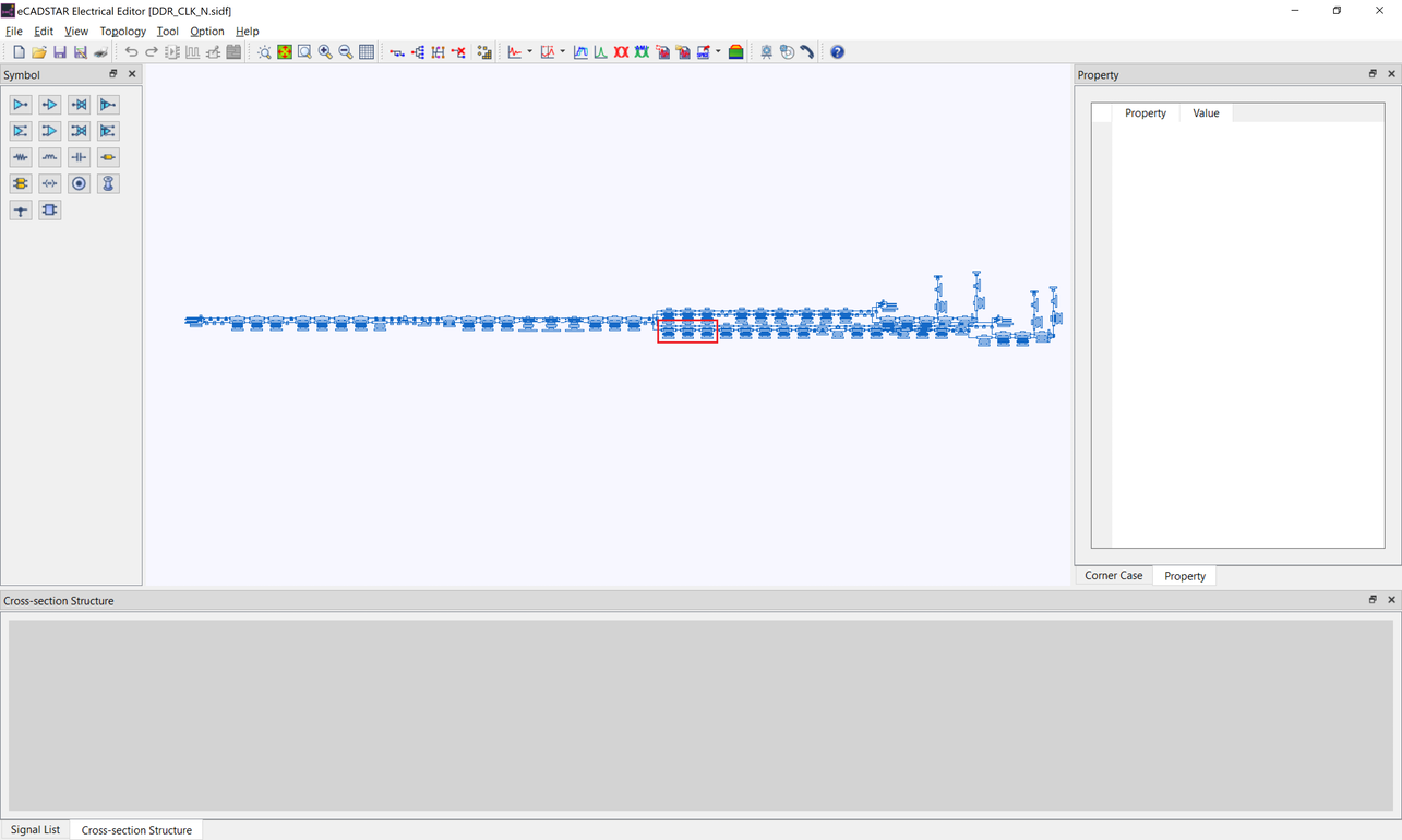
- In the Constraint Browser tree view, select differential pair "DDR_CLK_N" and click Utility > Extract Scenario on the menu bar. Electrical Editor starts, and displays the topology. As a result of enabling co-planar references, more transmission line symbols are in the topology than those displayed previously.
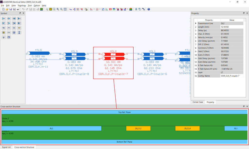
- On the eCADSTAR Electrical Editor canvas, select a differential line symbol in the extracted topology, and check the Cross-section Structure view.
Use
 Zoom Area to frame a section of the
topology containing coupled transmission line symbols.
Zoom Area to frame a section of the
topology containing coupled transmission line symbols.
The adjacent layers are detected as reference planes, and reference conductors in the same layer that also have the cutting plane structure of the detected differential signal.
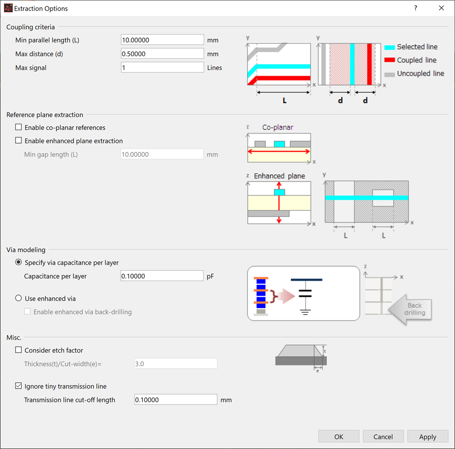
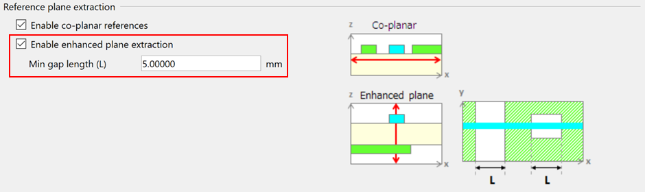
In the Reference plane extraction section, specify how to handle the reference plane to a signal track.
- Select File > Exit to close eCADSTAR Electrical Editor.
- In eCADSTAR PCB Editor, click the Analysis > SI > Extract Scenario pull down menu on the ribbon. Select Extraction Options to display the Extraction Options dialog.
- Select Enable enhanced plane extraction in the Reference plane extraction section, and specify "5" in the Min gap length (L) box.
- Click OK to close the dialog.
- In the Constraint Browser Tree view, select differential pair "DDR_CLK_N" and click Utility > Extract Scenario on the menu bar. Electrical Editor starts, and displays the topology. Note that more transmission line symbols are displayed because of enabling enhanced plane extraction.

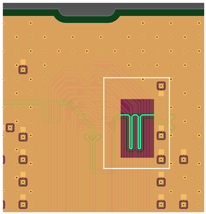
- On the eCADSTAR Electrical Editor canvas, zoom in to the area highlighted in the following image.
- Select a transmission line symbol that exceeds 11.00 mm and check the Cross-section Structure view.
This transmission line is the result of extracting the line routed in conductor layer 9.
The top reference plane is detected, but the bottom reference plane is not detected.
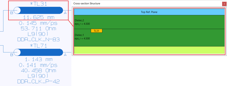
This cutting plane structure is due to a cutout that exists on conductor layer 10.
The topology extraction options include the following, as well as the reference plane extraction settings.
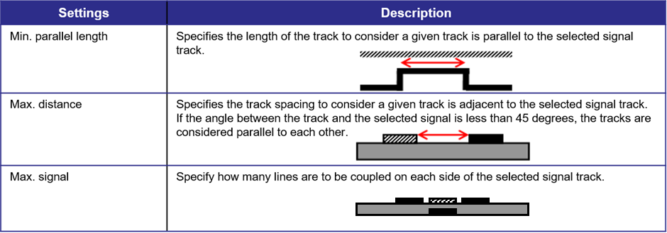
- Coupling criteria
- Via modeling
Coupling criteria
The conditions are described below for which signal tracks that are adjacent to a selected signal track are considered coupled.
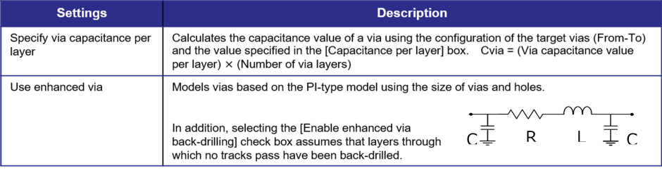
Via modeling
Procedures for handling via models are described below.
In eCADSTAR Electrical Editor, you can reference topology or simulator options for the target net.
- Select File > Exit to close eCADSTAR Electrical Editor.
This task is demonstrated in the following video.
