
Task 6: Defining Skew Groups
In this topic, you will define and constrain the Skew Groups that are required for this design.
- Using the MyHSDesign1.pdes design from the previous topic, launch Constraint Browser from the Home tab on the ribbon.
- In Constraint Browser, click
 Select All in the Signals
tab to select all the signals.
Select All in the Signals
tab to select all the signals. - In Constraint Browser, click
 Create Skew Group on the ribbon or
click Edit > Create Skew Group
on the menu. The Create Skew Group
dialog is launched.
Create Skew Group on the ribbon or
click Edit > Create Skew Group
on the menu. The Create Skew Group
dialog is launched.
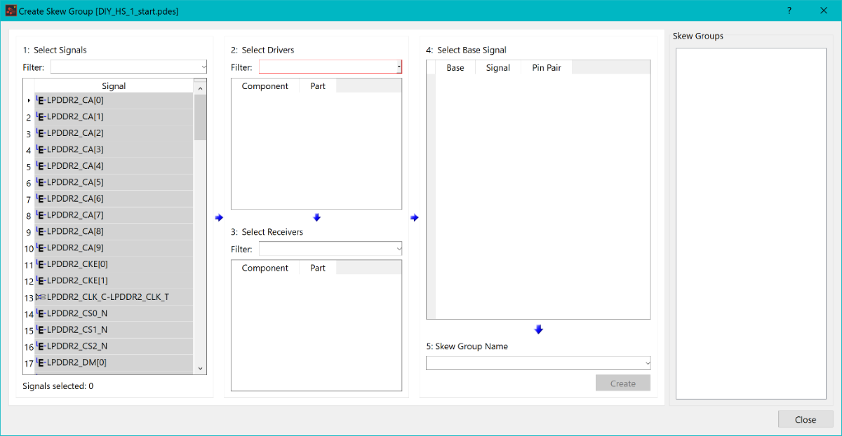
Figure 1: Create Skew Group Dialog
- In the 1: Select Signals section, select signals LPDDR2_CA[0-9] by dragging the cursor over the LPDDR2_CA[ ] signals to select them.
- Select the clock differential pair LPDDR2_CLK_C - LPDDR2_CLK_T by pressing Ctrl, and then clicking it. Components should now be displayed in the other fields in the dialog.
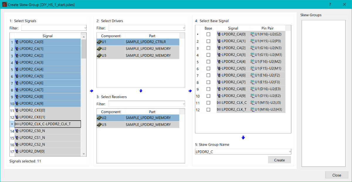
Figure 2: Create Skew Group Dialog
- In the 2: Select Drivers section, ensure that component U1 is selected.
- In the 3: Select Receivers section, ensure that component U2 is selected.
- In the 4: Select Base Signal section, select the Base column to specify the differential pair clock as the base signal.
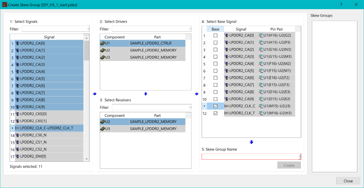
Figure 3: Create Skew Group Dialog
- In the 5: Skew Group Name section, define the name of the Skew Group as “CLK_TO_ADDRESS_U1-U2” and click Create. It is added to the Skew Groups section, on the right side of dialog.
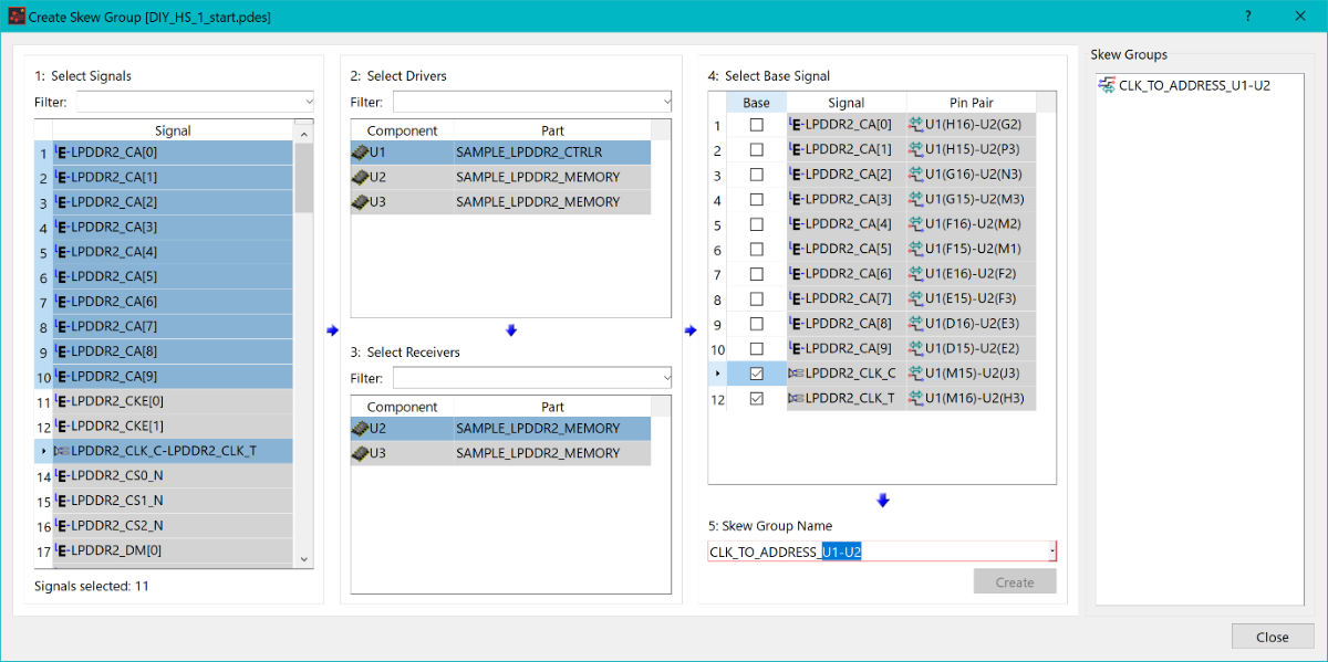
Figure 4: Create Skew Group Dialog
-
Using the above procedure, create the following skew groups.
| 1. Select Signals | 2. Select Drivers | 3. Select Receivers | 4. Select Base Signal | 5. Skew Group Name |
|---|---|---|---|---|
|
U1 | U3 | LPDDR2_CLK_C-LPDDR2_CLK_T (Differential Pair) | CLK_TO_ADDRESS_U1-U3 |
|
U1 | U2 | LPDDR2_DQ0S_C-LPDDR2_DQ0S_T (Differential Pair) | ByteLane0 |
|
U1 | U2 | LPDDR2_DQ0S_C-LPDDR2_DQ0S_T (Differential Pair) | ByteLane1 |
|
U1 | U2 | LPDDR2_DQ0S_C-LPDDR2_DQ0S_T (Differential Pair) | ByteLane2 |
|
U1 | U2 | LPDDR2_DQ0S_C-LPDDR2_DQ0S_T (Differential Pair) | Bytelane3 |
|
U1 | U2 | LPDDR2_DQ0S_C-LPDDR2_DQ0S_T (Differential Pair) | Bytelane4 |
|
U1 | U2 | LPDDR2_DQ0S_C-LPDDR2_DQ0S_T (Differential Pair) | Bytelane5 |
|
U1 | U2 | LPDDR2_DQ0S_C-LPDDR2_DQ0S_T (Differential Pair) | Bytelane6 |
|
U1 | U2 | LPDDR2_DQ0S_C-LPDDR2_DQ0S_T (Differential Pair) | Bytelane7 |
|
U1 | U2 | LPDDR2_DQ0S_C-LPDDR2_DQ0S_T (Differential Pair) | DQS_TO_CLK |
- Save the design, and close the Create Skew Group dialog.
The above procedures are demonstrated in the following video.
