
Checking Layer Configuration
Before performing EMI, PI or DC analysis, you must correctly set the parameters. These include layer thickness and resistivity. This topic describes this procedure.
- On the Start menu in Windows, click eCADSTAR > eCADSTAR [Version] > PCB Editor [Version]. eCADSTAR PCB Editor starts.
- In the File tab, click Open. Alternatively, click Open on the Home tab. The Open dialog is displayed.
- Browse to the following location and click Open: “C:\Users\Public\eCADSTAR\eCADSTAR [Version]\Analysis\PI_PCB\PI.pdes”.
Note
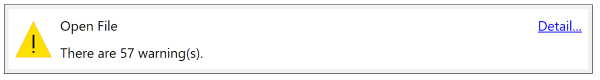
A warning message may be displayed when the design is opened. This is caused by eCADSTAR attempting to load 3D models from the analysis library, which has not yet been populated. This will not affect the operation of the analysis tools.
A warning message may be displayed when the design is opened. This is caused by eCADSTAR attempting to load 3D models from the analysis library, which has not yet been populated. This will not affect the operation of the analysis tools.
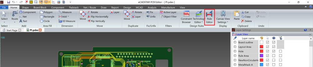
- On the ribbon, click Home > Design Rules > Rule Editor. The Rule Editor dialog is launched.
- Open the Board tab and check the definition settings.
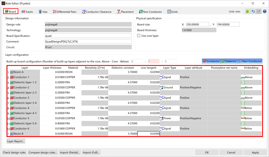
- Click OK to close the Rule Editor dialog.
This task is demonstrated in the following video.
