
Task 3: Creating User Defined Layers
In this section you will explore user defined layers. These layers can be added to a technology, at the technology library level, or locally within a PCB design. User defined layers are used as standalone layers for keepout definition, template definition, documentation or drawing purposes.
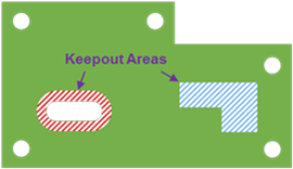
Figure 1: Standalone Layers for Documentation or Drawing Purposes
Task 3: Creating User Defined Layers
In this task, you will create user defined layers.
- Open the technology file DIY-4_Layer that was created earlier from the technology library. Select the Layer Configuration tab.
- Expand the associated layer list for “Conductor-1” by clicking ">".
- Right-click User defined layer. On the assist menu, click Add User Defined Layer. The Add User Defined Layer dialog is displayed.
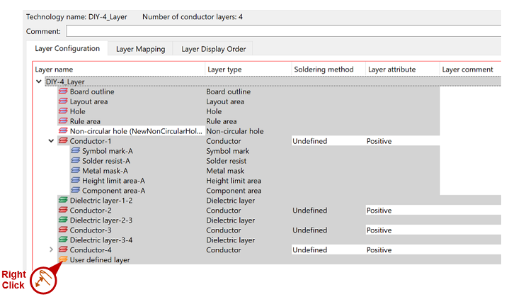
Figure 2: 4 Layer Technology File
- Enter “Top_Component_Keepout” in the Layer Name box and click OK.
Spaces are not permitted in user defined layer names. Using spaces creates an individual layer for each word. This allows you to quickly add multiple layers.
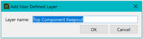
Figure 3: Add User Defined Layer Dialog
You have now added a user defined layer. Assign it as an inhibit (or keepout) layer as follows.
- Continue to use the technology file DIY-4_Layer, created earlier from the technology library.
- Select the Layer Configuration tab.
- Right-click on the user defined layer “Top_Component_Keepout”.
- On the assist menu, select Associate with Conductor Layer. The Specify Conductor Layer to Associate dialog is displayed.
- In the Specify Conductor Layer to Associate dialog, select the “Conductor-1” layer.
- Set the Layer Type as “Component Keepout”.
- Click Associate. Conductor-1 is now linked to a component keepout layer.
- Save the Technology Library. You have now successfully added an inhibit layer.
This task is demonstrated in the following video.
