
Symbol Mark Generation
In the PCB Cosmetics section, you will learn about the wide selection of tools that eCADSTAR contains that assist in the addition of non-electrical board items and manufacturing details. The following sections cover some of these tools.
Symbol Mark generation
Symbol Mark generation is used for automatically creating the reference designators on any layer defined as a “Symbol Mark” layer type. This could apply to a Symbol Mark or an assembly layer. The character width, spacing, line width, justification and position can be specified. Reference designators can be added to individual components or the whole side of the board. Once generated, reference designators can be moved and rotated as required. In addition to reference designators, part names or user-defined text can be generated.
Overview
- On the Draw tab, open the Component Symbol dialog.
- Change the required fields within the Component Symbol dialog.
- Select the component or components within the PCB layout area that require reference designator generation.
- Modify the reference designator position, as required.
Task 18: Creating Reference Designators (Symbol Mark Creation)
Reference designators are the names given to each component to identify it. In this task you will create reference designators on a Symbol Mark layer.
- If it is not already open, open the Design7.pdes design. Alternatively, use your own, completed design.
- Set the active layer to Symbol-A and display Conductor-1.

Figure 1: Setting the active layer to Symbol-A.
- On the Status bar, click Change
Object Filter
 . The Change Object Filter dialog
is displayed.
. The Change Object Filter dialog
is displayed.
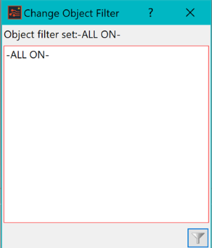
Figure 2: The Change Object Filter dialog.
- On the Change Object Filter dialog, click the bottom-right button to open the Object Filter dialog.
- Set the Object Filter dialog as shown below, and click Add to store the object filter settings with the name Comp_Symbols.
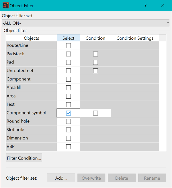
Figure 3: The Object Filter dialog.
- Close the Object Filter dialog.
- Perform a frame selection within the canvas with a click+drag operation from lower-left to upper-right of the design. All the Component Symbol marks on the active layer are selected.
- Press the Delete key to delete the Component Symbol marks from the design.
- On the eCADSTAR PCB Editor ribbon, select Draw > Text > Component Symbol. The Component Symbol dialog is displayed.
- Set the values shown below in the Component Symbol dialog.
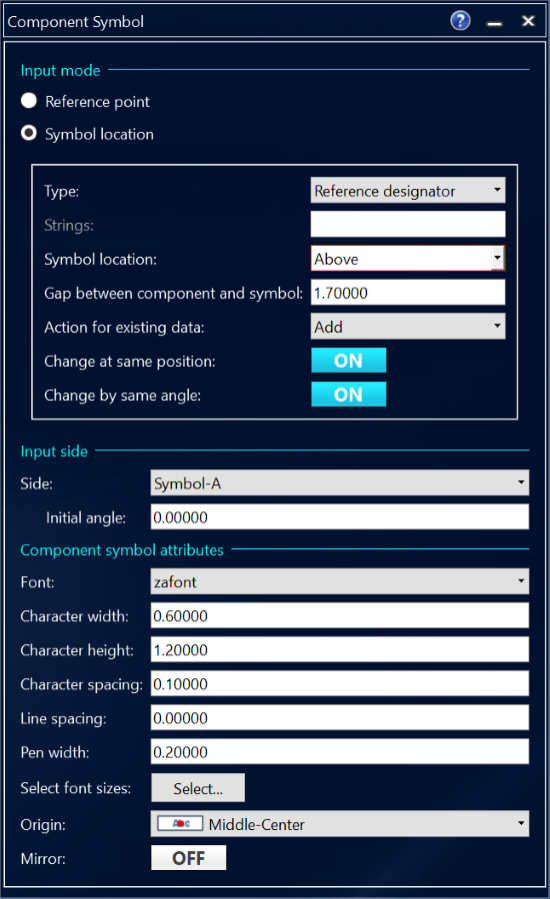
Figure 4: The Component Symbol dialog
- Ensure that the Object Filter is set to -ALL ON-.
- Click and hold the mouse at the top-left corner of R14, and drag down to the bottom-right of R16 to frame select the area as shown below.
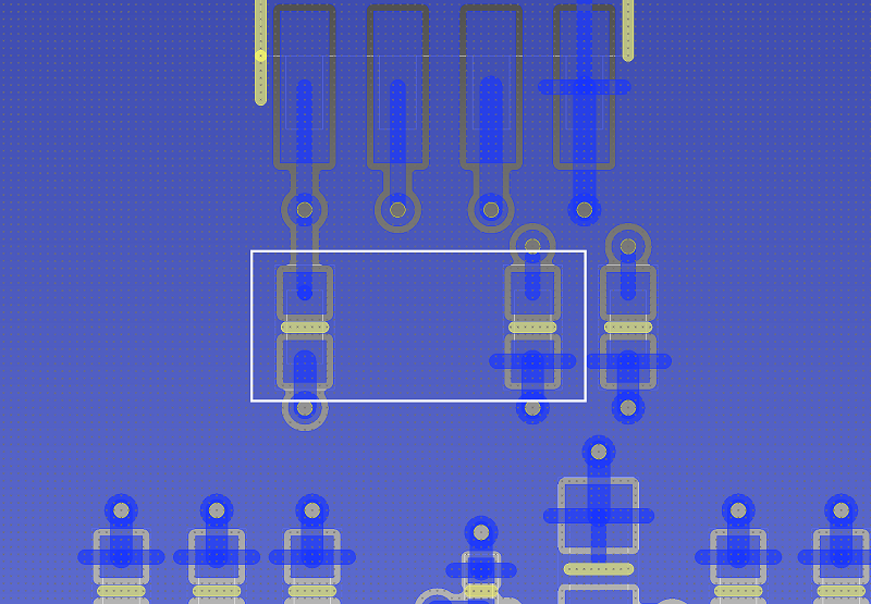
Figure 5: Framing an Area to Generate Reference Designators
When the area has been framed, the reference designators are automatically generated as shown below.

Figure 6: The Completed Reference Designators
The Symbol Mark can then be placed at the required location. To allocate reference designators to the whole board, select all components on the design.
You can move the generated text using the Move command, on the Home tab. A leader line is displayed when the text is moved. This shows the relationship between the generated text and the component.
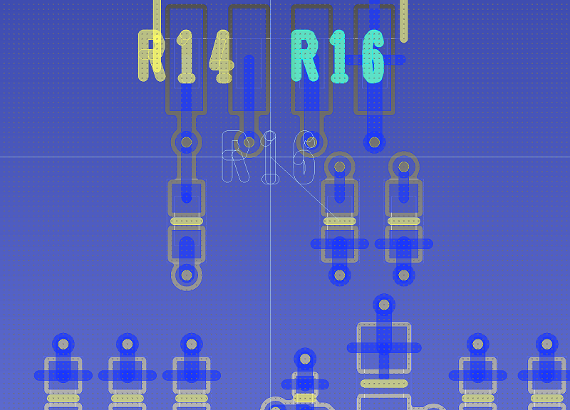
Figure 7: Leader line, shown when moving Reference Designators
This process can also be used to generate reference designators on the Assembly Layer. The Active layer must be set to Assembly-A.
Task 18 is demonstrated in the following video.
You have now allocated reference designators to the design. You will move on to cutting the symbol mark in the next section.
