
Task 2: Using eCADSTAR Symbol Editor
In this task, you will create a schematic symbol for the CD4093BM96 NAND integrated circuit. You will also create a schematic symbol for a six-pin plated through-hole or surface mount connector.
Creating a Symbol
- Open eCADSTAR Library Editor, if not already open.
- Select the Symbols tab.
- On the ribbon, click Home > Rows >
 Add
. The symbol name "NewSymbol-1" is created in the Symbol Name column.
Add
. The symbol name "NewSymbol-1" is created in the Symbol Name column. - Change the name "NewSymbol-1" to "DIY-NAND".
- Ensure that the new symbol is selected, and then click Home
> Edit >
 Symbol on the ribbon to open the Symbol Editor.
- In the displayed Warning dialog, click Yes.
- On the ribbon, click Home > Setting > Symbol Settings.
- In the Symbol Settings dialog, Size/Zone tab, set the properties shown below and click OK.
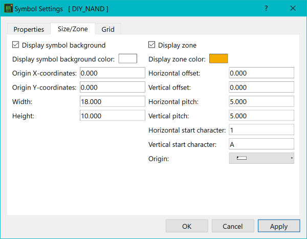
Figure 1: Setting Size/Zone Values
- In the Symbol Settings dialog, Grid tab, set the grid properties shown below.
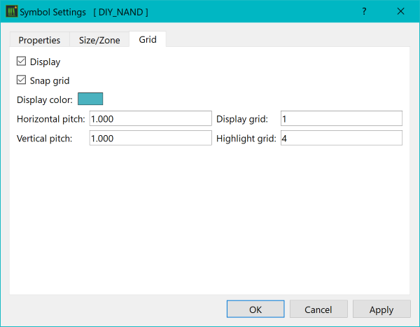
Figure 2: Setting the Grid
This procedure is demonstrated in the following video.
Drawing an Outline
To ensure that the outline is created successfully, you must complete all steps in this section as a continuous operation. Starting this task and then completing it at a later time will adversely affect subsequent tasks.
- On the Symbol Editor
ribbon, click Home > Shape >
 Polyline.
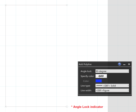
The Polyline dialog is displayed.
Polyline.
The Polyline dialog is displayed. - In the Polyline dialog, specify the values displayed below.
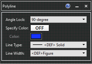
Figure 3 The Polyline Dialog
- Draw an outline as shown below by clicking at the four numbered points.
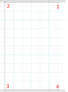
Figure 4: Drawing an Outline
An indicator will appear on the canvas when the current end point of the shape has a valid Angle Lock to the start point. This is defined in the command dialog.
- At point 4, right-click and select Insert Arc on the assist menu.
- Click the end point (Point 1 as shown below).
- Adjust the curvature to form a semi-circle by moving the cursor to the right. Click on canvas position to set the radius of the arc (Point 2 as shown below).
- Right-click and select Closed Shape on the assist menu. You have now created the body of the symbol.
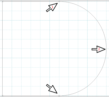
Figure 5: Symbol Outline
This procedure is demonstrated in the following video.
Adding the Inverter Symbol
- On the Symbol Editor
ribbon, click Home > Shape >
 Circle.
 - Click a center point, and drag outwards to create a circle.
- Click to define the radius of the circle.
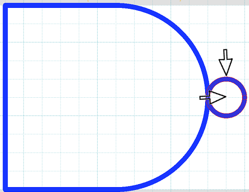
Figure 6: Adding the Inverter
- On the Symbol Editor
ribbon, click Home > Shape > Polyline.
- Add the connections and logic symbol to the symbol, as shown below. You can complete the action by double-clicking or selecting Finish from the assist menu.
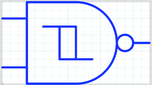
Figure 7: Adding Connections to the Symbol
Adjusting Sheet Size and Origin
- On the Symbol Editor ribbon, click Home > Setting > Fit to Data to adjust the sheet size to automatically fit around the size of the symbol, if it was not previously set as described in "Creating a Symbol" step 8.
- Click Home > Setting > Move Origin, and click the required position on the canvas to set the origin position of the symbol.
The above two procedures are demonstrated in the following video.
Adding Area Fills
- On the canvas, click the outline of the symbol to select it. The selected outline is shown below.
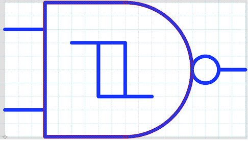
Figure 8 Selecting the Symbol Outline
- On the Symbol Editor ribbon, click Draw > Shape > Area Fill. The Area Fill dialog is displayed.
- In the Area Fill dialog, set Specify Color to ON.
- Click the Color button. The Select color dialog is displayed.
- In the Select color dialog, select the color shown in the image below and click OK. Select the canvas inside the selected outline. The symbol outline is filled using the specified color. Note that the area fill is partially transparent.
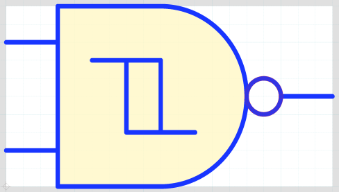
Figure 9 Specifying the color of an area fill.
- On the symbol, click the outline of the circle to select it.
- In the Area Fill dialog, set Specify color to OFF. Select the canvas inside the selected outline.
This procedure is demonstrated in the following video.
Adding Pins
- On the Symbol Editor ribbon, click Home > Pin > Add Pin.
- Click the ends of the connections to add pins 1, 2 and 3.
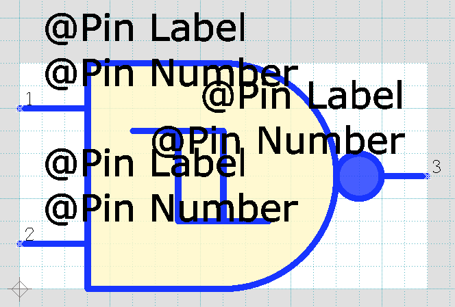
Figure 10: Adding Pin Numbers
When adding a new pin, a text field is placed on the canvas, by default, for the pin number and pin label. This text field will be filled later when mapped with the part footprint. Each text field can be moved, justified and deleted, based on your preference. Additionally, with any text object selected, the font size may be changed in the properties window.
Hiding Text Fields
- On the status bar, select Symbol Pin in the Object Filter box. This allows you to select pins on the canvas.
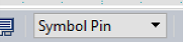
Figure 11: The Object Filter box
- On the canvas, click pin 1. The text fields that are associated with pin 1 are highlighted.
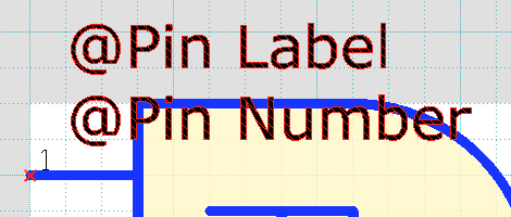
Figure 12: Text fields for Pin 1
- On the Status bar, ensure that the Properties
panel is displayed by clicking the
 button.
 - In the Properties panel, right-click the Pin Label field and select Hide Viewer on the assist menu.
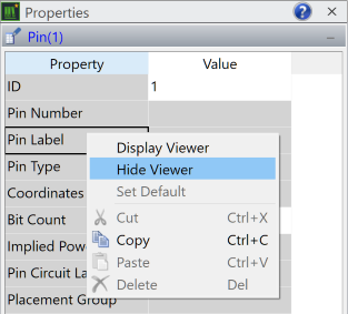
Figure 13: The Properties panel
- On the canvas, confirm that the @Pin Label text field is no longer displayed as part of the default symbol information.
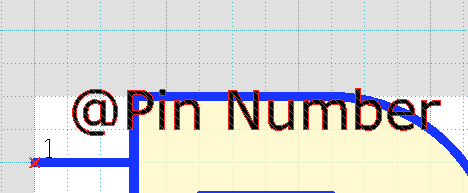
Figure 14: @Pin Label text field not displayed
- Hide the @Pin Label text field for the remaining two pins.
- Set the Object Filter to Property Viewer, and then change the justification using the Properties panel, Origin row.
- Move the pin property viewers to the positions shown below by dragging them. Click a position on the canvas to define their new location. Alternatively, select the property viewer on the canvas and then click Home > Move > Move on the ribbon. Click a position on the canvas to define its new location.
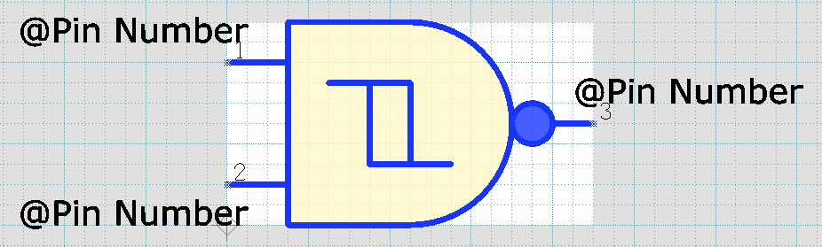
Figure 15: Adjusted pin property viewers
The above two procedures are demonstrated in the following video.
Adding Part Information using the Symbol Settings Dialog
- On the ribbon, click Home > Setting > Symbol Settings. The Symbol Settings dialog is displayed.
- In the Symbol Settings dialog, Properties tab, right-click the Reference Designator row.
- Select Display Viewer on the assist menu.
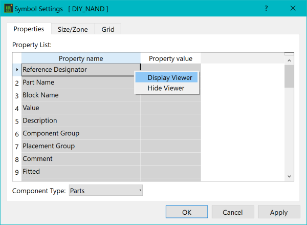
Figure 16: Symbol Settings dialog
- In the Symbol Settings dialog, Properties tab, right-click the Value row.
- Select Display Viewer on the assist menu.
- Close the Symbol Settings dialog by clicking the OK button.
- Adjust the part property viewers to the location shown in the image below.
- If there is a requirement to move the location of the property viewer positions, then set the Object Filter to Property Viewer.
- If there is no requirement to move the location of the property viewer positions, then reset the Object Filter to Main Object.
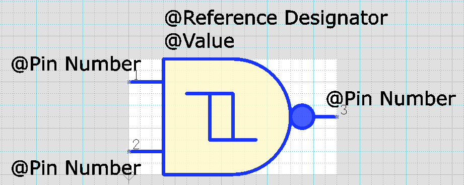
Figure 17: Completed symbol
- On the File menu, click Save to save the symbol.
- Close the symbol. You have now created a symbol for the NAND Gate.
This procedure is demonstrated in the following video.
Creating a Symbol for a Plated Through-hole, or Surface Mount Connector
It is optional to create this symbol, as it is already defined in the library with the name ‘CONN_SIL’. This enables you to progress further through the training.
- Open eCADSTAR Library Editor if not already open.
- Following the previous instructions, create a new symbol for the connector "DIY-CONN_SIL" using the Rectangle and Polyline commands. The method for adding the area fills is described below. The completed symbol is shown in the following image.
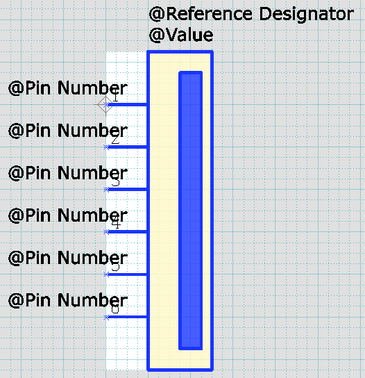
Figure 18: The Completed Plated Through-Hole Connector Symbol
- Using the Ctrl key, select both the outer and inner rectangles, and click Draw > Shape > Area Fill on the ribbon. The Area Fill dialog is displayed.
- In the Area Fill dialog:
- Set Specify Color to ON and select the required color by clicking the Color button.
- In the Fill Style box, select solid.
- On the canvas, click the white canvas area between the outer and inner rectangles. The area between the selected rectangles is filled.
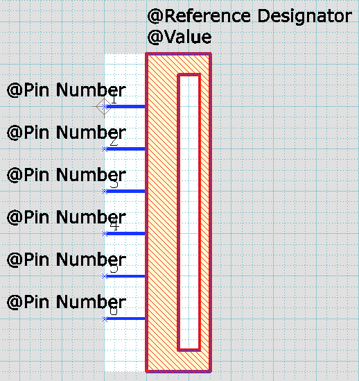
Figure 19: Outer Area Fill
- In the Area Fill dialog, set Specify Color to OFF.
- On the canvas, click the white canvas inside the inner rectangle. The inner rectangle is filled.
- Ensure to save the symbol by clicking Save on the File menu.
You have now built schematic symbols for both the CD4093BM96 NAND integrated circuit and for the above connector. The above connector is a generic 6 pin symbol could be used for a plated through-hole or surface mount connector. This procedure is demonstrated in the following video.
Alternate Symbols
Alternate symbols are different items that can be used with a part. They are often used if there is a different drawing standard requirement for the schematic. eCADSTAR allows you to assign alternate symbols to a part.
