
Task 8: Routing Branched Address Signals
In this topic, you will route the signals to topologies using the DIY_HS_1_Partial_Routed.pdes design. This design contains all the required Skew Groups.
- Open the partially routed design, DIY_HS_1_partially_routed.pdes. In this task, you will route one of the address signals.
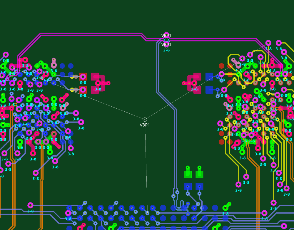
Figure 1: Unrouted Address Signal
- On the eCADSTAR PCB Editor ribbon, select View > Canvas > Routing Balloon. The Routing Balloon is displayed on the canvas.
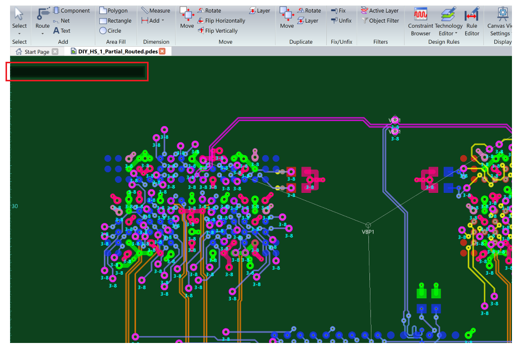
Figure 2: The Routing Balloon
- Click the routed Differential Pair. Some of the dependencies that are required to route it are displayed in the Routing Balloon. A red bar is displayed at the bottom of the Routing Balloon. This shows the maximum pin pair length of 45 mm that is set for the Differential Pair.
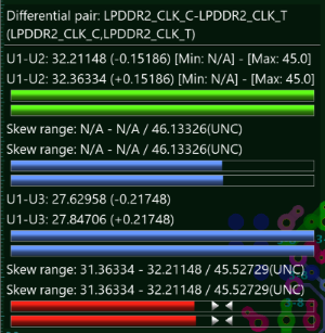
Figure 3: The Routing Balloon
- On the Status Bar, ensure that Conductor-3 is set as the active layer.
- On the canvas, deselect the differential pair that you selected.
- On the ribbon, select Net/Route > Routing > Add Route. The Add Route dialog is displayed.
- Start to route the unconnected net associated with the LPDDR2_CA[0] signal. Continue routing it until you reach the top point between the SDRAMS, shown below.
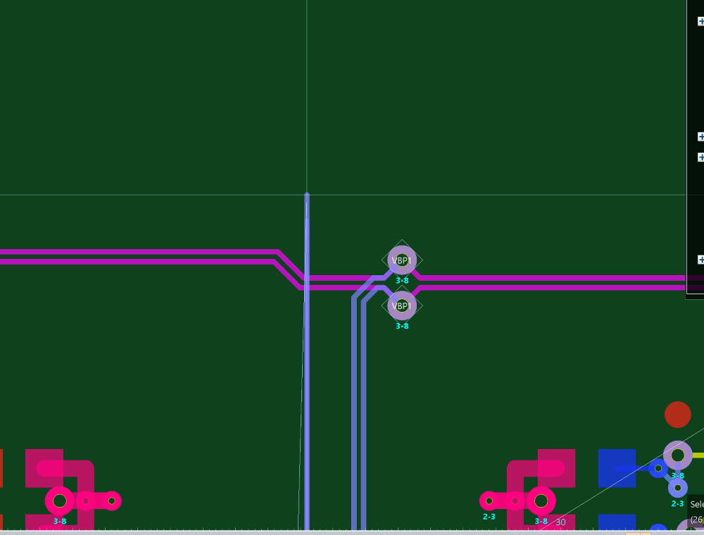
Figure 4: Routing an Unconnected Net
- Double-click the mouse to place a via. In the displayed Active Layer dialog, select "Conductor-7" or press "7" on the keyboard to set it as the active layer. A via is placed on the canvas.
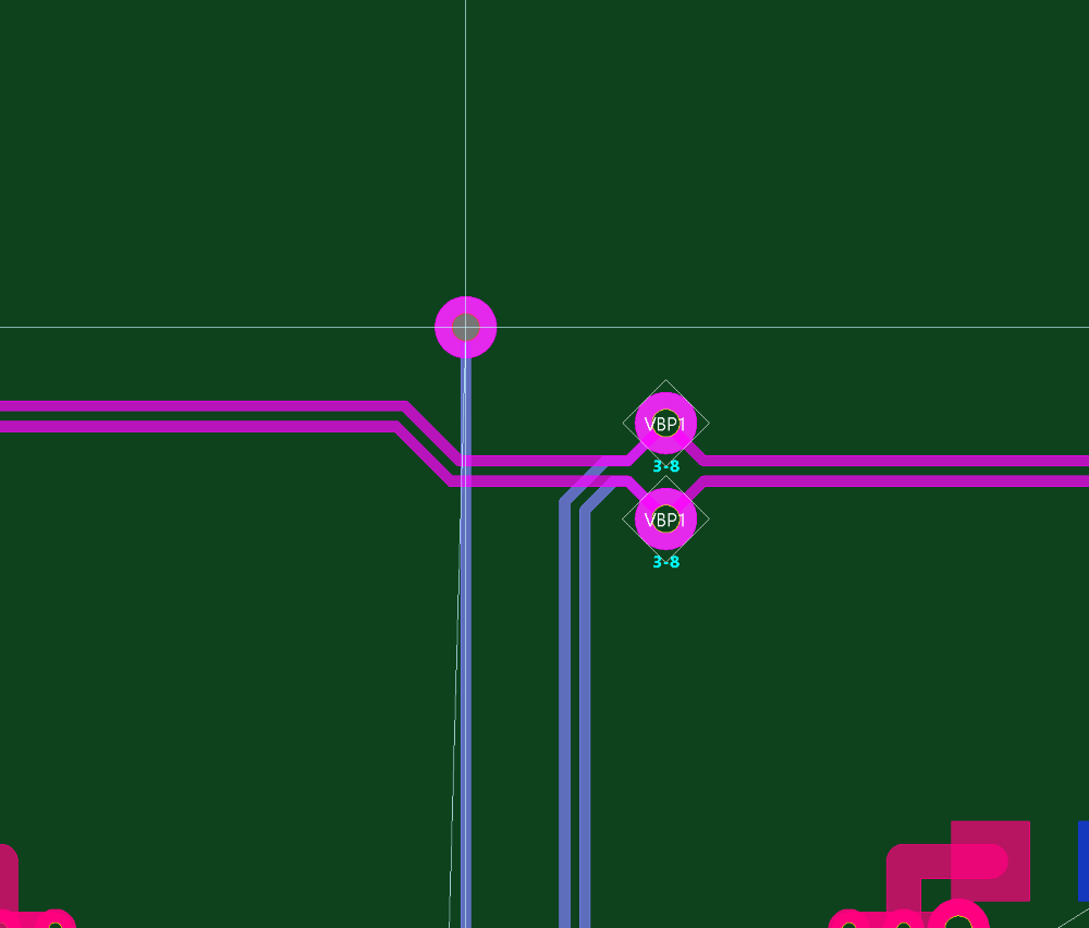
Figure 5: Placing a Via
- Right-click, and select Collect Next Virtual Branch Point on the assist menu. The virtual branch point will snap to the via.
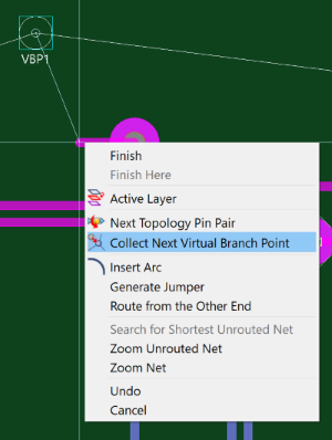
Figure 6: Collect Next Virtual Branch Point
You can then route either way from it.
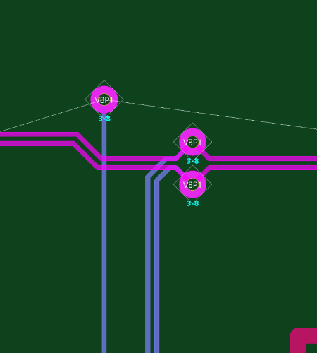
Figure 7: Routing from a Virtual Branch Point
Note
If you make an adjustment to the routing of a partially-routed net, then the virtual branch point may be disconnected from the via. The virtual branch point is then placed in a centralized position between the unrouted nets.
- Click the via to continue routing. The track is routed to the unconnected net marker on the right.
- Right-click, and select Next Topology Pin Pair on the assist menu. The pin pair that is currently being routed is switched, to route towards the memory module.
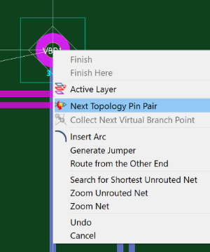
Figure 8: Routing to the Next Topology Pin Pair
- To finish routing the pin pair, continue routing to the first memory module.
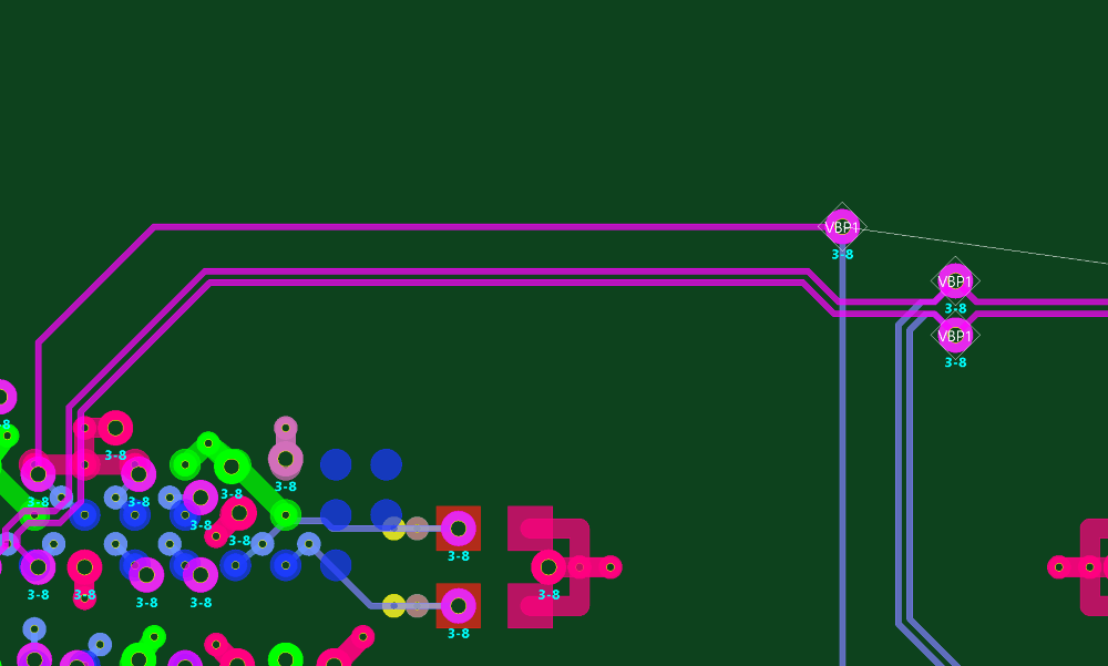
Figure 9: Routing to the First Memory Module.
- Finish routing the other pin pair to complete the routing of the LPDDR2_CA[0] signal.
- Save the design as MyHSDesign2.pdes. This completes the routing task for the High Speed training. Next you will lengthen the design to constraints.
The above procedures are demonstrated in the following video.
