
This topic describes the Signals
tab in the Constraint Browser,  Signals section. It also applies to Constraint Viewer. The values that you
specify override any values specified at a higher level in the Constraint
Browser: Signals section, Classes/Groups tab.
Signals section. It also applies to Constraint Viewer. The values that you
specify override any values specified at a higher level in the Constraint
Browser: Signals section, Classes/Groups tab.
- In eCADSTAR PCB Editor, launch Constraint Browser by clicking Design > Design Rules > Constraint Browser or, alternatively Home > Design Rules > Constraint Browser on the ribbon.
- In eCADSTAR PCB Viewer, launch Constraint Viewer by clicking Home > Design Rules > Constraint Viewer on the ribbon.
- In eCADSTAR Schematic Editor, launch Constraint Browser by clicking Design > Browser > Constraint or Home > Browser > Constraint on the ribbon.
- In eCADSTAR Schematic Viewer, launch Constraint Viewer by clicking Home > Constraint Viewer > Constraint Viewer on the ribbon.
If a particular column is displayed in the Signals tab and the Classes/Groups tab, then the relevant value is updated in both tabs. The following tabs are displayed in the pane on the right.
- Some tabs are displayed only when the environment is High Speed.
- The Lengthening and SI Measurement tabs are not displayed in Constraint Browser for eCADSTAR Schematic Editor.
- The SPICE tab is not displayed in Constraint Browser for eCADSTAR PCB Editor.
Lengthening (eCADSTAR PCB Editor)
Analysis (eCADSTAR PCB Editor)
Analysis (eCADSTAR Schematic Editor)
SI Measurement Tab (eCADSTAR PCB Editor)
SPICE Tab (eCADSTAR Schematic Editor)
In eCADSTAR PCB Editor, if you select Auto-update Constraint Browser when changing data in the PCB Editor: Application Settings, Interaction section, then values in Constraint Browser for eCADSTAR PCB Editor are automatically updated when you make relevant changes on the canvas. However, values in the Actual columns are not updated automatically. To update them, click Update values in Constraint Browser. Alternatively, click the Update Actual Values in Constraint Browser button on the ribbon. Add this command to the ribbon using the Ribbon Setting Dialog.
Signals Tab
The Signals tab, in the Signals section provides a view of your design at signal level. Signals are displayed in the Signals tree. Specify the items that are displayed using the Signal Type buttons or Filter box.
Signals Tree
Displays all signals, unless you apply filters. You can filter the displayed signals in this section before selecting the items that are added to the Signals table. Select multiple items using the CTRL or Shift keys, or by dragging the cursor.
You can view the items that comprise a signal by clicking the arrow next to the relevant item. For example, the pins, components and pin pairs can be displayed that are associated with a particular signal. Alternatively, right-click an item and select Expand or Collapse on the assist menu.
| Item | Description |
|---|---|
 Show/Hide E-Nets Show/Hide E-Nets
|
Displays or hides E-Nets in the tree. An E-Net is a set of one or more logical nets. E-Nets that contain more than one logical net are joined together via passive components. |
 Show/Hide differential
pairs Show/Hide differential
pairs |
Displays or hides differential pairs in the tree. |
 Show/Hide busses Show/Hide busses
|
Displays or hides busses in the tree. This button is not available in Constraint Browser for eCADSTAR Schematic Editor. |
 Show/Hide power/ground
nets Show/Hide power/ground
nets |
Displays or hides power and ground nets in the tree. |
| Filter box | Allows you to display signals whose name partially matches the text string that you enter. |
 Select all items Select all items
|
All items that are currently shown in the tree are displayed in the Signals table. |
Assist Menu
If you right-click a signal at the top level, then the following commands are available on the assist menu.
| Value | Description |
|---|---|
| Send Selection |
Displays and selects the specified object on the canvas.
See: Sending Selected Objects
to the Canvas. Note
The following should be considered when routing a differential pair that has a topology template assigned. In the Signals Tree, if you right-click the top level of the differential pair, and click Send Selection on the assist menu, then the entire differential pair is selected and displayed on the canvas. This allows you to start routing it using the Add Route command. However, when selecting a differential pair at this level, an incorrect Differential Pair Rule Stack may be applied to the transmission line which you start routing. This can create width and clearance errors in the routed tracks. To ensure that correct Differential Pair Rule Stacks are applied to each transmission line, follow one of these procedures.
|
| Create Pin Pair Routing Report | Displays the Pin Pair Routing Report dialog. This displays details for the pin pair routes between the components of the signal. |
| Create Differential Pair Coupling Report | Displays the Differential Pair Coupling Report dialog. This displays details for the coupled and non-coupled parts of differential pairs, and highlight them on the canvas. |
| Create Crosstalk Estimation Report | Displays the Crosstalk Estimation Report dialog. For a selected signal, the Crosstalk Estimation Report estimates the crosstalk effects that it receives from adjacent signals. Crosstalk voltages are estimated, and a report is created based on the coupling between tracks, and driver information. |
| Create Multiple Pin Pairs | Displays the Create Multiple Pin Pairs dialog. This allows you to create pin pairs for the selected signal. |
| Create Skew Group | Displays the Create Skew Group dialog. This allows you to create a skew group using signals that you select in the Signals Tree. |
| Net Group Manager | Displays the Net Group Manager dialog. This allows you to create, rename or delete net groups. It also allows you to add or remove E-Nets, power and ground nets from a selected net group. |
| Differential Pair Class Manager | Displays the Differential Pair Class Manager dialog. This allows you to create, rename or delete differential pair classes, and add or remove differential pairs from a selected differential pair class. |
| E-Net Class Manager | Displays the E-Net Class Manager dialog. This allows you to create, rename or delete E-Net classes, and add or remove E-Nets from a selected E-Net class. |
| Net Class Manager | Displays the Net Class Manager dialog. This allows you to create, rename or delete net classes, and add or remove nets from a selected net class. |
| Delete | Deletes the selected signal. |
| Expand | Displays the items that comprise a signal. For example, the pins, components and pin pairs can be displayed that are associated with a particular signal. Alternatively, click the arrow by an item in the Signals Tree. |
| Collapse | Collapses the items within an expanded view of a selected item. Alternatively, click the 'down' arrow by an item in the Signals Tree. |
View
Allows you to specify the items shown in the Signals table by filtering the contents of the Signals tree, and toggling the display of the Bus, Differential Pair and E-Net columns.
- If you click Select all items
in the Signals tree, all currently-displayed
items in the tree are shown in the Signals
table.
| Item | Description | |
|---|---|---|
| View list | Allows you to define the items that are shown in the Signals table. This is done by filtering the items listed in the Signals tree by setting a type of item, or specifying that only selected items in the tree are shown. | |
| Selected | Only items that are currently selected in the Signals tree are displayed in the Signals table. | |
| E-Net | For the items selected in the tree, the contents of the Signals table are filtered to only display E-Nets. | |
| Net | For the items selected in the tree, the contents of the Signals table are filtered to only display nets. | |
| Pin Pair | For the items selected in the tree, the contents of the Signals table are filtered to only display pin pairs. | |
| Component | For the items selected in the tree, the contents of the Signals table are filtered to only display components. | |
| Pin | For the items selected in the tree, the contents of the Signals table are filtered to only display pins. | |
|
Show/Hide bus column
|
Toggles the display of the Bus
column for each tab in the Signals
table. This button is not available in Constraint Browser for eCADSTAR Schematic Editor. |
|
|
Show/Hide differential
pair column |
Toggles the display of the Differential Pair column for each tab in the Signals table. | |
|
Show/Hide E-Net column
|
Toggles the display of the E-Net column for each tab in the Signals table. |
Update simulation status
To view previous simulation results, select the relevant signals the Tree view, and then click Update simulation status. A timestamp is displayed in the Simulation Status column for any signals that have results available. Clicking the ellipsis in one of these cells will launch the ARV with the results.
Update values
The Signals table is updated with the values in the relevant design. Alternatively, click the Update Actual Values in Constraint Browser button on the ribbon. Add this command to the ribbon using the Ribbon Setting Dialog.
The Update values button is not available in Constraint Browser for eCADSTAR Schematic Editor.
You can also specify that values in Constraint Browser are automatically updated when you make relevant changes on the canvas. Do this by selecting Auto-update Constraint Browser when changing data in the PCB Editor: Application Settings, Interaction section. Note that values in the Actual columns are not updated automatically.
Reconstruct E-Net
If an operation that changes the connections of nets is performed, or a net or bus label is changed, then clicking Reconstruct E-Net will reconstruct the structure of the E-Net. In Constraint Browser for eCADSTAR PCB Editor, this button is located in the Utility menu and on the toolbar.
Basic Tab
Displays values for the items selected in the Signals tree. The specified items are displayed in the Selected column. Select multiple items using the Ctrl or Shift key, or by dragging the cursor. By default, the following columns are displayed. The Customize Table Configuration Dialog allows you to display additional columns in this table. These items can be filtered using the View list, and by clicking <Filter> in each column. Columns that are colored gray cannot be edited.
| Item | Description | |
|---|---|---|
| Bus | Displays the buses that you select in the Signals
tree. Select multiple buses using the Ctrl
or Shift key, or by dragging the
cursor. Toggle the display of this column by clicking in the View
section.This column is
not available in Constraint Browser for eCADSTAR Schematic Editor. |
|
| Differential Pair | Displays the differential pairs that you select in the Signals tree. Select multiple differential
pairs using the Ctrl or Shift key, or by dragging the cursor. Toggle
the display of this column by clicking in the
View section. |
|
| E-Net | Displays the E-Nets that you select in the Signals
tree. Select multiple E-Nets using the Ctrl
or Shift key, or by dragging the
cursor. Toggle the display of this column by clicking in
the View section. |
|
| Selected | Displays the item that you select in the Signals tree. Select multiple items using the Ctrl or Shift key, or by dragging the cursor. | |
| Signal | Where appropriate, the signal is displayed that is associated with the items selected in the Signals tree. | |
| Color | Specify the display color of the item that is displayed in
the Selected column. This value
is displayed in the Signals
tab and Classes/Groups
tab in Constraint Browser when you enter it.
Select a color in the displayed Select
color dialog and click OK.
This dialog is displayed by pointing the cursor at the Color
column, and then clicking the displayed Note
|
|
| Voltage (V) | For E-Nets and nets, specify the voltage that is used for simulation purposes. The value that you specify is displayed in this column in the Signals tab and Classes/Groups tab in Constraint Browser. | |
| Part / Part Name | Displays the part name associated with a component displayed in the Selected column. | |
| Pin Count |
Displays the number of pins on the item displayed in the Selected column. This column is not available in Constraint Browser for eCADSTAR Schematic Editor. |
|
| Value | Displays the value associated with the item that you select in the Signals tree. | |
| Pin Name / Pin Label | Displays the names of the pins that are associated with a signal. | |
| Pin Type |
Displays the pin type of the selected item. This column is not available in Constraint Browser for eCADSTAR Schematic Editor. |
|
 INPUT INPUT
|
Indicates that the selected item is an input pin. | |
 OUTPUT OUTPUT
|
Indicates that the selected item is an output pin. | |
 BIDIRECT BIDIRECT
|
Indicates that the selected item is a bidirectional pin. | |
 POWER POWER
|
Indicates that the selected item is a power pin. | |
 GROUND GROUND
|
Indicates that the selected item is a ground pin. | |
 NC NC
|
Indicates that the selected pin is not connected. | |
| Comment | Displays the comment that you associate with the selected item. This value is also displayed in the Properties Panel. |
Design Rule Tab
Displays Design Rule values for the items selected in the Signals tree. Values are displayed for each item in the Selected column. The Customize Table Configuration Dialog allows you to display additional columns in this table. These items can be filtered using the View list, and by clicking <Filter> in each column. Columns that are colored gray cannot be edited.
| Item | Description | |
|---|---|---|
| Bus | Displays the buses that you select in the Signals
tree. Select multiple buses using the Ctrl
or Shift key, or by dragging the
cursor. Toggle the display of this column by clicking in the View
section. This column is not available in Constraint Browser for eCADSTAR Schematic Editor. |
|
| Differential Pair | Displays the differential pairs that you select in the Signals tree. Select multiple differential
pairs using the Ctrl or Shift key, or by dragging the cursor. Toggle
the display of this column by clicking in the
View section. |
|
| E-Net | Displays the E-Nets that you select in the Signals
tree. Select multiple E-Nets using the Ctrl
or Shift key, or by dragging the
cursor. Toggle the display of this column by clicking in
the View section. |
|
| Selected | Displays the item that you select in the Signals tree. Select multiple items using the Ctrl or Shift key, or by dragging the cursor. | |
| Track Width | Allows you to specify a rule stack that you created in the Rule library. Values are displayed in the Signals tab and Classes/Groups tab in Constraint Browser when you enter them. | |
| Track Width Stack | For E-Nets and nets that you select in the Signals
tree, specify a Track Width Stack from the Rule library. These
are created in the Tracks tab in the
Rule Editor dialog. Select a value in the Rule
Stack dialog. This dialog displayed by pointing the cursor in
this column, and then clicking the displayed  button.
Note
|
|
| Differential Pair Rule Stack | For a differential pair, specify a differential pair rule stack
from the Rule library. These are created in the Rule
Editor Dialog: Differential Pairs Tab. Select a value in the
Rule Stack dialog. This dialog displayed
by pointing the cursor in this column, and then clicking the displayed
button. |
|
| Topology Template | Allows you to assign a compatible
topology template to the E-Net or differential pair that you select
in the Signals tree. This can
be done using the Assign
Topology Template dialog, or by specifying
its name in the Topology Template
column. This column is only available in a High Speed environment.
Click in this column to display the Assign Topology Template dialog.
You can also copy and paste an existing value
in this column. If you attempt to specify an incompatible value,
then a warning message is shown, and the value is not updated.
An incompatible value may have a topology structure which does
not match the selected E-Net or differential pair. For example,
it may comprise a different number of ICs or passive components.
When you enter a compatible topology template,
it is automatically checked. If the topological structure of the
relevant signal does not follow the assigned topology template,
then the value in this column is shown in red. The topology template
is also checked whenever the following actions are performed.
When the topological structure of the signal matches the assigned topology template, the value in this column is immediately shown in black. This column is not available in Constraint Browser for eCADSTAR Schematic Editor. Note If an invalid topology is assigned to a differential pair, then the topology is shown with a yellow triangle. This may occur if the E-Net construction has changed since the template was assigned. In this case, the widths and spacings defined in the topology are not considered. Instead, the standard widths and spacings for the differential pair are used. 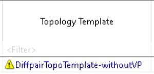 |
|
| Clearance | Specify a clearance class and rule stacks. These are created in the Clearance Class Manager dialog and the Rule Editor dialog, Conductor Clearance tab, respectively. Values are displayed in the Signals tab and Classes/Groups tab in Constraint Browser when you enter them. | |
| Clearance Class | For a signal that you select in the Signals
tree, specify a clearance class that you created in the Clearance
Class Manager dialog. Select a value in the displayed Clearance Class Dialog dialog. The Clearance
Class Manager dialog is displayed by clicking
Utility > Clearance Class Manager
in the Constraint Browser menu. The value that you select is also displayed in the Clearance Class row in the Properties Panel in eCADSTAR Schematic Editor. Note In eCADSTAR PCB Editor, you can forward annotate the clearance classes that you specify in Constraint Browser for eCADSTAR Schematic Editor. Select Load clearance rules in the design in the Forward Annotation dialog. |
|
| Same Net Design Rule Stack | For the signals that you select in the Signals
tree, specify a Same Net Design Rule Stack from the Rule library.
This defines the clearance that is applied, by default, between
conductors with the same net. These are created in the Rule
Editor dialog, Conductor Clearance
tab, Conductor
sub tab. Select a value in the Rule
Stack dialog. This dialog displayed by pointing the cursor in
this column, and then clicking the displayed
button.
Note In eCADSTAR PCB Editor, you can forward annotate the Same Net Design Rule Stacks that you specify in Constraint Browser for eCADSTAR Schematic Editor. However, in eCADSTAR Schematic Editor, you cannot back annotate the Same Net Design Rule Stacks that you specify in Constraint Browser for eCADSTAR PCB Editor. |
|
| Hole/Area Design Rule Stack | For the signals that you select in the Signals
tree, specify a Hole/Area Design Rule Stack from the Rule library.
This defines the minimum clearances between holes and layout areas,
and conductor types. These are created in the Rule
Editor dialog, Conductor Clearance
tab, Hole/Area
sub tab. Select a value in the Rule
Stack dialog. This dialog displayed by pointing the cursor in
this column, and then clicking the displayed
button.
Note In eCADSTAR PCB Editor, you can forward annotate the Hole/Area Design Rule Stacks that you specify in Constraint Browser for eCADSTAR Schematic Editor. However, in eCADSTAR Schematic Editor, you cannot back annotate the Hole/Area Design Rule Stacks that you specify in Constraint Browser for eCADSTAR PCB Editor. |
|
| Shielding | Allows you to configure a shield pattern, and assign it to
a net in the Signals table.
Values are displayed in the Signals
tab and Classes/Groups
tab in Constraint Browser when you enter them.
|
|
| Mode | Select from the following shield pattern modes: OFF: shielding is not added around the relevant track. If shielding is set for an E-Net, this setting allows you to turn it off for a constituent net. Same Layer: shielding is added on the same layer around the track. Same/Adjacent Layers: shielding is added on the same layer and on adjacent layers around the track. Adjacent Layers: shielding is only added on adjacent layers around the track. |
|
| Net name | Using the Net selector dialog, specify the signal name of the shield pattern. You can narrow down the signals displayed in the dialog by selecting or clearing the GND, Power and Signals check boxes, and by filtering the displayed values using the Net name box. | |
| Track Width Stack | Specify a Track Width Stack from the Rule library. These are
created in the Rule Editor
Dialog: Tracks Tab. Select a value in the Rule
Stack dialog. This dialog displayed by pointing the cursor in
this column, and then clicking the displayed
button. |
|
| Gap | Specify the clearance between the shield pattern and the track. | |
| Voltage Difference Clearance | Allows you to specify voltages for a signal, and override the
voltage difference clearance values that are set in the Rule Editor, Conductor
Clearance: Voltage Difference tab.
Note Clearance rules for creepage can also be set in the Conductor Clearance: Voltage Difference Tab and the Default Design Rule Stack section in Rule Editor. Clearance values are checked using the Creepage Check command, and the results are displayed in the Creepage Check Results dialog. The effective values for conductor clearance are set in the Clearance Priority section of the Rule Editor dialog. This defines the creepage values that are checked by the Creepage Check command. When the voltage difference between conductors is calculated, the Creepage results in the Creepage Check Results dialog are affected by the Phase Group, Low Voltage and High Voltage attributes as follows.
The largest difference is set as the Voltage difference value in the Creepage Check Results dialog.
|
|
| Voltage | Specify the voltage of the selected signal. The appropriate clearance is applied to the signal by referring to the Voltage difference clearance table section in the Rule Editor, Conductor Clearance: Voltage Difference tab, for the specified voltage. You can optionally specify values for Low Voltage and High Voltage. This may change the Voltage Difference Clearance table that is used. | |
| Low Voltage | If you specify values for Low Voltage and High Voltage, then the difference between the low voltage of one Net or E-Net and the high voltage of the next Net or E-Net is considered the greatest potential difference between the Nets or E-Nets of the signals. This determines the Voltage Difference Clearance table that is used, and overrides the setting in the Rule Editor, Conductor Clearance: Voltage Difference tab. | |
| High Voltage | If you specify values for Low Voltage and High Voltage, then the difference between the low voltage of one Net or E-Net and the high voltage of the next Net or E-Net is considered the greatest potential difference between the Nets or E-Nets of the signals. This determines the Voltage Difference Clearance table that is used, and overrides the setting in the Rule Editor, Conductor Clearance: Voltage Difference tab. | |
| Phase Group Name | Allows you to optionally define the name of the phase group associated with the selected signal. Specify an alphanumeric value. | |
| Table Stack | Allows you to override the default clearance table stack that
is applied to the design in the Rule
Editor, Conductor
Clearance: Voltage Difference tab. Select a value in the Rule Stack dialog. This dialog displayed by pointing the cursor in this column, and then clicking the displayed
button.
If you do not select a value, then the default clearance table
stack is applied. |
Routing Tab
Displays Routing values for the items selected in the Signals tree. For each item in the Selected column, values are displayed in the Signals tab and Classes/Groups tab in Constraint Browser. The Customize Table Configuration Dialog allows you to display additional columns in this table. These items can be filtered using the View list, and by clicking <Filter> in each column. Columns that are colored gray cannot be edited.
| Item | Description | |
|---|---|---|
| Bus | Displays the buses that you select in the Signals
tree. Select multiple buses using the Ctrl
or Shift key, or by dragging the
cursor. Toggle the display of this column by clicking in the View
section. This column is not available in Constraint Browser for eCADSTAR Schematic Editor. |
|
| Differential Pair | Displays the differential pairs that you select in the Signals tree. Select multiple differential
pairs using the Ctrl or Shift key, or by dragging the cursor. Toggle
the display of this column by clicking in the
View section. |
|
| E-Net | Displays the E-Nets that you select in the Signals
tree. Select multiple E-Nets using the Ctrl
or Shift key, or by dragging the
cursor. Toggle the display of this column by clicking in
the View section. |
|
| Selected | Displays the item that you select in the Signals tree. Select multiple items using the Ctrl or Shift key, or by dragging the cursor. | |
| Total Length | When you click Update values, the total routing length is displayed for a selected E-Net or net. This column is not available in Constraint Browser for eCADSTAR Schematic Editor. | |
| Track Width | Allows you to select a Track Width Stack that you created in
the Rule library. The length of track can then be calculated whose
width is outside the values specified by the rule stack. This column is not shown in Constraint Browser for eCADSTAR Schematic Editor. |
|
| Track Width Stack | Select a Track Width Stack from the Rule library. These are
created in the Rule Editor
Dialog: Tracks Tab. Select a value in the Rule
Stack dialog. This dialog displayed by pointing the cursor in
this column, and then clicking the displayed
button.
Note The value that you specify is shown in the Pin Pair Routing Report dialog. However, it is not adhered to by the Add Route or Autoroute commands. |
|
| Violated Length | For a selected E-Net or net, the length of track is displayed
whose width is outside the values defined in the specified track
width stack. This is selected in the Track
Width Stack column. Click Update
values to display the Violated
Length value. This column is not available in Constraint Browser for eCADSTAR Schematic Editor. |
|
| Unrouted Net Count | Displays the number of unrouted nets for a selected signal.
This value is displayed in the Signals
tab and Classes/Groups
tab in Constraint Browser when you click Update
Values. This column is not available in Constraint Browser for eCADSTAR Schematic Editor. |
|
| Max. Via Count | Allows you to specify a maximum number of vias for a selected signal. If the calculated number of vias for the signal exceeds this value, then it is displayed in red in the Via Count column. | |
| Via Count | The calculated number of vias for a selected item. If this exceeds the Max Via Count value, it is displayed in red. This column is not available in Constraint Browser for eCADSTAR Schematic Editor. | |
| Allow Ring | Allows you to specify nets which are exempt from the Ring Removal function when manual routing. If Allow Ring is selected for a net in Constraint Browser, then setting Ring Removal to ON has no effect for the 45, 90 and Free routers only. | |
| No. of required Testpoints | Shows the number of testpoints for a selected net, and allows
you to specify a value. You can set a value for this column in
the Routing tab in either the Signals
tab or Classes/Groups
tab in Constraint Browser. The value is automatically set
in both locations when you enter it. This column is not available in Constraint Browser for eCADSTAR Schematic Editor. |
|
| Net Layer | For a selected net, you can specify the conductor layers on
which it can be routed on using the Autorouter.
Select the required conductor layers in the displayed Net
Layer dialog. Display this dialog by pointing the cursor
at this cell and then clicking the button.
You can set a value for this column in the Routing
tab in either the Signals
tab or Classes/Groups
tab in Constraint Browser. The value is automatically set
in both locations when you enter it. This column is not available
in Constraint Browser for eCADSTAR Schematic Editor. |
High Speed Routing Tab
Displays High Speed routing values for the items selected in the Signals tree. For each item in the Selected column, values are displayed in the Signals tab and Classes/Groups tab in Constraint Browser. The Customize Table Configuration Dialog allows you to display additional columns in this table. These items can be filtered using the View list, and by clicking <Filter> in each column. Columns that are colored gray cannot be edited. This tab is only available in a High Speed environment.
| Item | Description | |
|---|---|---|
| Bus | Displays the buses that you select in the Signals
tree. Select multiple buses using the Ctrl
or Shift key, or by dragging the
cursor. Toggle the display of this column by clicking in the View
section. This column is not available in Constraint Browser for eCADSTAR Schematic Editor. |
|
| Differential Pair | Displays the differential pairs that you select in the Signals tree. Select multiple differential
pairs using the Ctrl or Shift key, or by dragging the cursor. Toggle
the display of this column by clicking in the
View section. |
|
| E-Net | Displays the E-Nets that you select in the Signals
tree. Select multiple E-Nets using the Ctrl
or Shift key, or by dragging the
cursor. Toggle the display of this column by clicking in
the View section. |
|
| Selected | Displays the item that you select in the Signals tree. Select multiple items using the Ctrl or Shift key, or by dragging the cursor. | |
| Pin Pair Length | For the E-Net, net, differential pair or pin pair that you select in the Signals tree, this section allows you to specify the required minimum and maximum distance between the pin pairs. | |
| Min. | For the E-Net, net or pin pair that you select in the Signals tree, specify the required minimum distance between the pin pairs. Specify a value that is greater than 0, and less than or equal to 20000. | |
| Max. | For the E-Net, net or pin pair that you select in the Signals tree, specify the required maximum distance between the pin pairs. Specify a value that is greater than 0, and less than or equal to 20000. | |
| Actual | If you select a pin pair in the Signals
tree, then its length in the design is displayed when you click
Update values. If the displayed value is outside of the minimum or maximum values
that you specify for the relevant E-Net, net or pin pair, then
it is displayed in red. See Creating
Multiple Pin Pairs. This column is not
available in Constraint Browser for eCADSTAR Schematic Editor.
Note The actual routed length of the pin pair is shown, rather than the manhattan length. |
|
| Pin Pair Delay | For the E-Net that you select in the Signals
tree, this section allows you to specify the minimum and maximum
delay that is permitted between the pin pairs.
Note In Constraint Browser for eCADSTAR PCB Editor, delay is displayed in either nanoseconds or picoseconds, depending on the value specified in the Delay section, in the Application Settings dialog, Interaction tab. You must restart Constraint Browser to apply changes to this setting. In Constraint Browser for eCADSTAR Schematic Editor, the predefined delay units are displayed. |
|
| Min. | For the E-Net that you select in the Signals tree, specify the minimum delay that is permitted between the pin pairs. | |
| Max. | For the E-Net that you select in the Signals tree, specify the maximum delay that is permitted between the pin pairs. | |
| Actual | For a pin pair that you select in the Signals tree, the calculated propagation delay is displayed when you click Update values. This value is calculated based on the pin pair lengths in the design. See Creating Multiple Pin Pairs.This column is not available in Constraint Browser for eCADSTAR Schematic Editor. | |
| Characteristic Impedance | For the E-Net or net that you select in the Signals tree, this section allows you to specify the minimum and maximum characteristic impedance. | |
| Min (Ω) | For the E-Net or net that you select in the Signals tree, specify the minimum characteristic impedance. | |
| Max(Ω) | For the E-Net or net that you select in the Signals tree, specify the maximum characteristic impedance. | |
| Match Ratio (%) |
For the total length of the E-Net or net that you select in the Signals tree, the percentage is displayed which is within the minimum and maximum impedance values that you specify. When you click Update values, characteristic impedance is calculated using the layer stack and material values in the design. The match ratio is not displayed if the minimum and maximum values of the characteristic impedance are not set. This column is not available in Constraint Browser for eCADSTAR Schematic Editor. |
Signal Class Tab
Displays Signal Class values for the items selected in the Signals tree in the pane on the left. Values are displayed for each item in the Selected column. Select multiple items using the CTRL or Shift keys, or by dragging the cursor. The Customize Table Configuration Dialog allows you to display additional columns in this table. These items can be filtered using the View list, and by clicking <Filter> in each column. Columns that are colored gray cannot be edited.
| Item | Description |
|---|---|
| Bus | Displays the buses that you select in the Signals
tree. Select multiple buses using the Ctrl
or Shift key, or by dragging the
cursor. Toggle the display of this column by clicking in the View
section. This column is not available in Constraint Browser for eCADSTAR Schematic Editor. |
| Differential Pair | Displays the differential pairs that you select in the Signals tree. Select multiple differential
pairs using the Ctrl or Shift key, or by dragging the cursor. Toggle
the display of this column by clicking in the
View section. |
| E-Net | Displays the E-Nets that you select in the Signals
tree. Select multiple E-Nets using the Ctrl
or Shift key, or by dragging the
cursor. Toggle the display of this column by clicking in
the View section. |
| Selected | Displays the item that you select in the Signals tree. Select multiple items using the Ctrl or Shift key, or by dragging the cursor. |
| Net Class | Using the Net class dialog, specify a net class that you created in the Net Class Manager dialog. This is accessed by clicking Edit > Net Class Manager in the Constraint Browser dialog. |
| E-Net Class | Using the E-Net class dialog, specify an E-Net class that you created in the E-Net Class Manager dialog. This is accessed by clicking Edit > E-Net Class Manager in the Constraint Browser dialog. |
| Differential Pair Class | Using the Differential pair class dialog, specify a differential pair class that you created in the Differential Pair Class Manager dialog. |
Differential Pair Routing Tab
For each item in the Selected column, differential pair routing values are displayed in the Signals tab and Classes/Groups tab in Constraint Browser. The Customize Table Configuration Dialog allows you to display additional columns in this table. Select multiple items using the CTRL or Shift keys, or by dragging the cursor. The Customize Table Configuration Dialog allows you to display additional columns in this table. These items can be filtered using the View list, and by clicking <Filter> in each column. Columns that are colored gray cannot be edited. This tab is only available in a High Speed environment.
| Item | Description | |
|---|---|---|
| Bus | Displays the buses that you select in the Signals
tree. Select multiple buses using the Ctrl
or Shift key, or by dragging the
cursor. Toggle the display of this column by clicking in the View
section. This column is not available in Constraint Browser for eCADSTAR Schematic Editor. |
|
| Differential Pair | Displays the differential pairs that you select in the Signals tree. Select multiple differential
pairs using the Ctrl or Shift key, or by dragging the cursor. Toggle
the display of this column by clicking in the
View section. |
|
| E-Net | Displays the E-Nets that you select in the Signals
tree. Select multiple E-Nets using the Ctrl
or Shift key, or by dragging the
cursor. Toggle the display of this column by clicking in
the View section. |
|
| Selected | Displays the item that you select in the Signals tree. Select multiple items using the Ctrl or Shift key, or by dragging the cursor. | |
| Differential Pair Rule | For a differential pair that you select in the Signals
tree, select a differential pair rule stack in the displayed Differential Pair Rule Stack dialog.
Display this dialog by pointing the cursor at this cell, and then
clicking the displayed button. |
|
| Differential Pair Rule Stack | For a differential pair that you select in the Signals
tree, select a differential pair rule stack from the Rule library.
Select a value in the displayed Differential
Pair Rule Stack dialog. This dialog displayed by pointing the
cursor at this cell, and then clicking the
button. Differential pair rule stacks are created in the Rule
Editor Dialog: Differential Pairs Tab. |
|
| Violated Length for Differential Rule |
For a selected differential pair, the total length of routes is displayed that violate the specified differential pair rule stack. This is displayed when you click Update Values. This column is not available in Constraint Browser for eCADSTAR Schematic Editor. |
|
| Match Ratio for Differential Rule (%) |
For all routes in a selected differential pair, the percentage of their total length is displayed that does not violate the specified differential pair rule stack. This column is not available in Constraint Browser for eCADSTAR Schematic Editor. |
|
| Differential Pair | Allows you to display the total length of routes in a selected differential pair. You can also display the total length that meets or does not meet the coupling criteria, and the percentage of routes that do meet them. You can also specify how close the signals in a differential pair are routed to each other. This section is not available in Constraint Browser for eCADSTAR Schematic Editor. | |
| Total Length | When you click Update Values, the total length is displayed of all routes in the differential pair. | |
| Coupled Length | For the differential pair, the total length of routes is displayed that meet the track spacing requirements for differential pairs. These requirements are set in the Track spacing column in the Rule Editor Dialog: Differential Pairs Tab. | |
| Non-coupled Length | For the differential pair, the total length of routes is displayed that do not meet the track spacing requirements for differential pairs. These requirements are set in the Track spacing column in the Rule Editor Dialog: Differential Pairs Tab. | |
| Coupled Ratio (%) | For the total length of routes in a differential pair, the percentage is displayed which meet the track spacing requirements for differential pairs. These requirements are set in the Track spacing column in the Rule Editor Dialog: Differential Pairs Tab. | |
| Length Difference between Positive/Negative | Allows you to specify the maximum difference in length that is permitted between the positive and negative tracks of the differential pair. The value in the design for this attribute is also displayed when you click Update values. | |
| Max. | Specify the maximum difference in length that is permitted between the positive and negative tracks of the differential pair. Specify a value that is greater than 0, and less than or equal to 20000. | |
| Actual |
When you click Update values, the maximum difference in length between the positive and negative tracks of the differential pair is displayed. If this value is greater than the value specified in the Max. field, then it is shown in red. This column is not available in Constraint Browser for eCADSTAR Schematic Editor. |
|
| Differential Impedance | Allows you to specify minimum and maximum values for the differential impedance of the differential pair. If you specify values for Min (Ω) and Max (Ω), then the Violated Length value is automatically displayed when you click Update values. | |
| Min (Ω) | Specify the minimum differential impedance value that is permitted for the differential pair. | |
| Max (Ω) | Specify the maximum differential impedance value that is permitted for the differential pair. | |
| Violated Length | For the differential pair routes, the total length is displayed that violates the differential impedance value in the design. If values are entered for Min (Ω) and Max (Ω), then the Violated Length value for the relevant design is displayed when you click Update values. This column is not available in Constraint Browser for eCADSTAR Schematic Editor. | |
| Match Ratio (%) | For the differential pair, the percentage of the routes is displayed that does not violate the differential impedance value in the design. When you click Update values, differential impedance is calculated using the layer stack and material values in the design. The match ratio is not displayed if the minimum and maximum values of the differential impedance are not set. This column is not available in Constraint Browser for eCADSTAR Schematic Editor. |
Lengthening Tab (eCADSTAR PCB Editor)
For the E-Net that you select in the Signals tree in Constraint Browser for eCADSTAR PCB Editor, these settings allow you to override the lengthening settings that are specified in the Design Settings dialog, Lengthen section. By default, the values specified in this section are used for the selected E-Net. However, you can override these values using the assist menu of the Lengthen command. Select multiple E-Nets using the Ctrl or Shift key, or by dragging the mouse. These items can be filtered using the View list, and by clicking <Filter> in each column. Columns that are colored gray cannot be edited.
This tab is not displayed in Constraint Browser for eCADSTAR Schematic Editor.
| Item | Description | |
|---|---|---|
| Bus | Displays the buses that you select in the Signals
tree. Select multiple buses using the Ctrl
or Shift key, or by dragging the
cursor. Toggle the display of this column by clicking in the View
section. |
|
| Differential Pair | Displays the differential pairs that you select in the Signals tree. Select multiple differential
pairs using the Ctrl or Shift key, or by dragging the cursor. Toggle
the display of this column by clicking in the
View section. |
|
| E-Net | Displays the E-Nets that you select in the Signals
tree. Select multiple E-Nets using the Ctrl
or Shift key, or by dragging the
cursor. Toggle the display of this column by clicking in
the View section. |
|
| Selected | Displays the item that you select in the Signals tree. Select multiple items using the Ctrl or Shift key, or by dragging the cursor. | |
| Meander Mode | For a selected E-Net or E-Net class, specify the meander mode that is used to lengthen the E-Net. The value that you specify is used in preference to the value specified in the Design Settings dialog, Lengthen section. | |
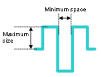
| Accordion | The following meander mode is used to lengthen the E-Net. The
maximum size and minimum space, shown below, can be specified
in this tab.
|
|
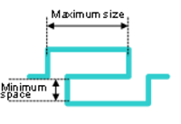
| Trombone | The following meander mode is used to lengthen the E-Net. The
maximum size and minimum space, shown below, can be specified
in this tab.
|
|
| Edge Style | For a selected E-Net or E-Net class, this setting allows you to specify the angle of the segment end of the lengthen pattern. The value that you specify is used in preference to the value specified in the Design Settings dialog, Lengthen section. | |
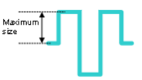
| Chamfer | The angle of the route segment end of the lengthen pattern
is set to 45 degrees. This is illustrated below for the Accordion meander mode.
|
|
| Square | The angle of the route segment end of the lengthen pattern
is set to 90 degrees. This is illustrated below for the Accordion meander mode.
|
|
| Semicircle | The angle of the route segment end of the lengthen pattern
is set to an arc. This is illustrated below for the Accordion meander mode.
|
|
| Max. Size | For a selected E-Net or E-Net class, set the maximum length
applied between parallel routes when lengthening a routing
pattern. The value that you specify is used in preference to the
value specified in the Design
Settings dialog, Lengthen
section. This is illustrated below for the Accordion
meander mode.
|
|
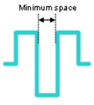
| Min Space | For a selected E-Net or E-Net class, set the minimum space
applied between parallel routes when lengthening a routing pattern.
The value that you specify is used in preference to the value
specified in the Design
Settings dialog, Lengthen
section. This is illustrated below for the Accordion
meander mode.
|


Analysis Tab (eCADSTAR PCB Editor)
For the item that you select in the Signals tree in Constraint Browser for eCADSTAR PCB Editor, this tab allows you to configure the analysis settings.
| Item | Description | ||||||||||||||||||||||||||||
|---|---|---|---|---|---|---|---|---|---|---|---|---|---|---|---|---|---|---|---|---|---|---|---|---|---|---|---|---|---|
| Bus | Displays the buses that you select in the Signals
tree. Select multiple buses using the Ctrl
or Shift key, or by dragging the
cursor. Toggle the display of this column by clicking in the View
section. |
||||||||||||||||||||||||||||
| Differential Pair | Displays the differential pairs that you select in the Signals tree. Select multiple differential
pairs using the Ctrl or Shift key, or by dragging the cursor. Toggle
the display of this column by clicking in the
View section. |
||||||||||||||||||||||||||||
| E-Net | Displays the E-Nets that you select in the Signals
tree. Select multiple E-Nets using the Ctrl
or Shift key, or by dragging the
cursor. Toggle the display of this column by clicking in
the View section. |
||||||||||||||||||||||||||||
| Selected | Displays the item that you select in the Signals tree. | ||||||||||||||||||||||||||||
| Stimulus | Select a signal, and click .
The Stimulus
dialog is displayed. This allows you to configure digital
stimuli, and add or delete user stimulus files. |
||||||||||||||||||||||||||||
| Simulation Status | Displays a timestamp for any signals that have results available. This is displayed by selecting the relevant signals in the Tree view, and then clicking Update simulation status. | ||||||||||||||||||||||||||||
| Pin Count | Displays the number of pins for the item that you select in the Signals tree. | ||||||||||||||||||||||||||||
| Value | Displays any attributes that are associated with a component that you select in the Signals tree. | ||||||||||||||||||||||||||||
| Device Name | Allows you to select a device model from the displayed dialog.
The device model that you select is displayed.
Note There may be a delay when this is done for the first time. |
||||||||||||||||||||||||||||
| Vendor | Displays the vendor associated with the selected device model. | ||||||||||||||||||||||||||||
| Nominated Driver | Allows you to specify that a component or pin is a driver by selecting the associated check box. | ||||||||||||||||||||||||||||
| Model Name | Displays the pin buffer model that is assigned to the relevant
pin. This value is added when you create a new PCB design. It
is also added to the Analysis tab
in the Constraint
Browser: Component/Parts Section, Components Tab.
To ensure that the displayed information is current,
perform a Simulation Library Reload.
This is required if you:
Note If there are any failed pin assignments, these are listed when you execute the Simulation Library Reload command after selecting a model for the first time. |
||||||||||||||||||||||||||||
| Model Type | Displays the type of pin buffer model that is assigned to the
relevant pin. The following types are supported in eCADSTAR.
Note If there are any failed pin assignments, these are listed when you execute the Simulation Library Reload command after selecting a model for the first time. |
Analysis Tab (eCADSTAR Schematic Editor)
For the item that you select in the Signals tree in Constraint Browser for eCADSTAR Schematic Editor, this tab allows you to configure the analysis settings.
| Item | Description |
|---|---|
| Differential Pair | Displays the differential pairs that you select in the Signals tree. Select multiple differential
pairs using the Ctrl or Shift key, or by dragging the cursor. Toggle
the display of this column by clicking in the
View section. |
| E-Net | Displays the E-Nets that you select in the Signals
tree. Select multiple E-Nets using the Ctrl
or Shift key, or by dragging the
cursor. Toggle the display of this column by clicking in
the View section. |
| Selected | Displays the item that you select in the Signals tree. |
| Stimulus | Select a signal, and click .
The Stimulus
dialog is displayed. This allows you to configure digital
stimuli, and add or delete user stimulus files. |
| Pin Count | Displays the number of pins for the item that you select in the Signals tree. |
| Value | Displays any attributes that are associated with a component that you select in the Signals tree. |
| Device Name | Allows you to select a device model from the displayed dialog.
The device model that you select is displayed.
Note There may be a delay when this is done for the first time. |
| Vendor | Displays the vendor associated with the selected device model. |
SI Measurement Tab (eCADSTAR PCB Editor)
For the item that you select in the Signals
tree in Constraint Browser for eCADSTAR PCB Editor,
this tab allows you to configure the SI measurement settings.
One or several signals can be selected on the SI Measurement tab. With the SI Measurement tab in front, if the Update values button is pressed:
- a standard SI simulation is carried out for all selected nets,
- specific automatic measurements are carried out on all signals for driver and receiver pins, and
- the results are displayed in the SI Measurement tab table in the Constraint Browser.
This tab is not displayed in Constraint Browser for eCADSTAR Schematic Editor.
| Item | Description | |
|---|---|---|
| Bus | Displays the buses that you select in the Signals
tree. Select multiple buses using the Ctrl
or Shift key, or by dragging the
cursor. Toggle the display of this column by clicking in the View
section. |
|
| Differential Pair | Displays the differential pairs that you select in the Signals tree. Select multiple differential
pairs using the Ctrl or Shift key, or by dragging the cursor. Toggle
the display of this column by clicking in the
View section. |
|
| E-Net | Displays the E-Nets that you select in the Signals
tree. Select multiple E-Nets using the Ctrl
or Shift key, or by dragging the
cursor. Toggle the display of this column by clicking in
the View section. |
|
| Selected | Displays the item that you select in the Signals tree. | |
| Max. Voltage (V) |
Max Voltage (Vmax) is the maximum positive voltage at the measured pulse of a signal with respect to 0.0 V. See Displaying the Maximal Voltage. |
|
| Rise/Fall Time (20%-80%) |
Rise |
Rise Time (20% - 80%) is the transition time from 20% to 80% of the signal swing between the simulated DC low and DC high level. See Displaying the Rise- and Fall Times. |
| Fall | Fall Time (20% - 80%) is the transition time from 80% to 20% of the signal swing between the simulated DC high and DC low level. See Displaying the Rise- and Fall Times. | |
| Slew Rate | The receiver Slew Rate is derived under setup conditions. Slew rates are the fraction of a specific voltage difference and the corresponding slope in (V/ns), i.e. r = V / t. See Displaying
the Slew Rate (Setup). Depending on the available receiver threshold values originating from the IBIS model, the slew rates are calculated and displayed under dynamic receiver threshold conditions. |
|
| Rise (V/ns) | Slew Rate Rise and Fall results are shown for e-nets and receiver pin in volts per nanosecond (V/ns). | |
| Fall (V/ns) | Slew Rate Rise and Fall results are shown for e-nets and receiver pin in volts per nanosecond (V/ns). | |
| Flight time | Rise and Fall | The Flight Time Rise/Fall is the time difference calculated between a receiver signal and a reference driver signal at specific thresholds or reference voltages. See Displaying the Flight Times. The maximum typical flight times with reference to Vth_(min|max) are calculated if corresponding receiver threshold parameters are available. |
| Total Cap. Load (pF) | On a per e-net base the Total Capacitive Load (C_total) is calculated as: C_total = C_Tx + C_Rx + C_Pkg + C_TL + C_Via + C_Passive with:
Note There are elements adding capacitive load which are not counted, e.g. IdEM models. |
|
| Crossing Voltage | Rise and Fall | The crossing voltage is the voltage at the crossing point of the measured pulses of the individual signals with respect to the supply voltage levels: (VICC + VISS) / 2. See Displaying the Crossing Voltage of Differential Pair Signals. |
| Spread (V) |
The Crossing Voltage Spread is the absolute value of the difference of the Crossing Voltage Rise and the Crossing Voltage Fall: VIcross_spread = | VIcross_rise – VIcross_fall | |
|
| Probe Location SI | The probe location for signal integrity analysis results, either PIN or DIE. These locations are specified within the IBIS file of a device. The Simulation Library Manager allows the values to be manually modified on the Device Data tab of a selected device. Note When no package data is present at a device, the default probe location is PIN. |
|
| Probe Location Timing | The probe location for flight time analysis results, either PIN or DIE. The following Timing Probe Locations combinations exits:
These locations are specified within the IBIS file of a device. The Simulation Library Manager allows the values to be manually modified on the Device Data tab of a selected device. Note When no package data is present at a device, the default probe location is PIN. |
SPICE Tab (eCADSTAR Schematic Editor)
Displays the SPICE component values for the items selected in the Signals tree in Constraint Browser for eCADSTAR Schematic Editor. Values are displayed for each item in the Selected column. These items can be filtered by clicking <Filter> in each column. Rows that are colored gray cannot be edited.
This tab is not displayed in Constraint Browser for eCADSTAR PCB Editor.
| Item | Description |
|---|---|
| Differential Pair | Displays the differential pairs that you select in the Signals tree. Select multiple differential
pairs using the Ctrl or Shift key, or by dragging the cursor. Toggle
the display of this column by clicking in the
View section. |
| E-Net | Displays the E-Nets that you select in the Signals
tree. Select multiple E-Nets using the Ctrl
or Shift key, or by dragging the
cursor. Toggle the display of this column by clicking in
the View section. |
| Selected | Displays the item that you select in the Signals tree. |
| SPICE OP Voltage | The Operating Point voltage for the selected net on the schematic sheet. This is simulated by the LTspice application. Operating Point voltage is used for analog simulation control units. Use it to set a voltage value to create adjusted results from calculations. |
| Item | Description |
|---|---|
 (Always send
selection) (Always send
selection) |
The object you select in a Constraint Browser is selected on the Canvas in both the eCADSTAR PCB Editor and eCADSTAR Schematic Editor and in any instance of Constraint Browser. |
 Toggle
Coupling Analysis Toggle
Coupling Analysis
|
If toggled on, then signals that meet the criteria for being coupled are extracted when you extract a scenario in Constraint Browser. During simulation, this allows you to see the effects of them being in close proximity. Specify coupling criteria in the Extraction Options dialog. |
| Message | Displays messages that are relevant to the changes that you make in Constraint Browser. |
| Units | In Constraint
Browser for eCADSTAR Schematic Editor,
the predefined measurement units are displayed. In Constraint
Browser for eCADSTAR PCB Editor,
the measurement units and delay units are displayed
that you specify. Set the measurement units in
eCADSTAR PCB Editor
as follows.
|
Constraint Browser: Signals section, Classes/Groups tab
Constraint Browser: Skew Groups Section
Constraint Browser: Component/Parts Section, Components Tab
Constraint Browser: Component/Parts Section, Parts Tab
Displaying Constraints and Attributes of Signals
Constraint Browser: Components Section
Constraint Browser
Constraint Viewer
Clearance Class Dialog
Attributes that are Forward and Back Annotated in eCADSTARFiltering Displayed Values in eCADSTAR TablesFiltering Displayed Values in eCADSTAR Tables
