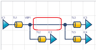
The Tracks tab in the Rule Editor dialog allows you to configure design rules for routing. The contents of the tab are described below.
Default track width stack
| Item | Description |
|---|---|
| Default track width stack | Allows you to select a track width stack that is displayed in the Track width stack box. The value that you select is referenced, by default, on the board. If Minimum copper width is defined by Track width stack is selected in the PCB Editor: Application Settings, Area fill section, then this value defines the minimum copper width of the area fills that you create. However, you can override this setting by assigning a different track width stack in the Design Rule tab, Track Width Stack column in the Constraint Browser: Signals section, Signals Tab or Constraint Browser: Signals section, Classes/Groups tab. This is a mandatory setting. |
Track width stack
Allows you to set the track widths for each conductor layer, and then calculate the characteristic impedance and delay associated with the specified values. Alternatively, you can calculate the track width, characteristic impedance and delay, based on a target impedance value that you specify.
| Item | Description |
|---|---|
| Track width stack box | Allows you to create a track width stack by typing its name and clicking Add. Multiple track width stacks can be created simultaneously by entering multiple names, separated by a space. This is a mandatory setting. |
| Add | Moves the track width stacks that you enter in the Track width stack box to the Track width stack list, below. |
| Track width stack list | Displays the track width stack names that you enter by clicking Add. |
| Calculate characteristic impedance -> Track Width | Displays the Calculate characteristic impedance -> Track Width dialog. This allows you to enter a value for target impedance. The track width, characteristic impedance and delay can then be calculated in this dialog, and the Tracks tab updated. |
| Calculate characteristic impedance | Calculates the characteristic impedance and delay, based on the values for Track width that you enter, as well as the thickness and the number of dielectric and conductor layers. The calculated values are displayed in the Track width stack table. |
Track width stack Table
| Item | Description | |
|---|---|---|
| Conductor layer | Shows the conductor layers that are added in the Board tab. | |
| Track width | Typical | Set the normal track width and press Return. This track width is used by default, and is a mandatory setting. |
| Minimum | Optionally, set the minimum track width that is permitted and press Return. This allows escape routing from surface-mount pads that are smaller than the Normal Track Width value. | |
| Maximum | Optionally, set the maximum track width that is permitted and press Return. | |
| Characteristic impedance [Ω] | The characteristic impedance associated with the track width that you specify. This value is calculated for each conductor layer when you click Calculate characteristic impedance, and added automatically to the Track width stack Table. This value is also produced by clicking Calculate characteristic impedance -> Track Width, and using the Calculate characteristic impedance -> Track Width to calculate it from a target impedance value. This is an optional setting. | |
| Delay | The delay per unit length, in nanoseconds, associated with the track width that you specify. This value is calculated for each conductor layer when you click Calculate characteristic impedance, and added automatically to the Track width stack Table. This value is also produced by clicking Calculate characteristic impedance -> Track Width, and using the Calculate characteristic impedance -> Track Width to calculate it from a target impedance value. This is an optional setting. This column is displayed only if delay is set to nanoseconds in the in . | |
You must restart Rule Editor to apply changes to the units for delay that you specify in the Application Settings dialog, Interaction tab.
Routing direction
Allows you to optionally set the preferred routing direction for each conductor layer. If you select X or Y in the Routing direction column, then these values are used by the Autoroute and Autorouter commands. If you select any other values, then they are ignored by these commands, and are displayed only to indicate the preferred direction for manual routing.
If you select X or Y in the Routing direction column, then you must close and then reopen the design before this value is used by the Autoroute command.
| Item | Description | |
|---|---|---|
| Conductor layer | Lists the conductor layers that are added in the Rule Editor Dialog: Board tab. | |
| Routing direction | Undefined | The preferred routing direction is not defined. If selected, then the value Unbiased (From Design) is displayed in the Layers dialog, Apparent Layers section. This dialog is accessed from the Routing Strategy dialog. |
| X | The preferred routing direction is in the X dimension. This value is used by the Autoroute and Autorouter commands. If selected, then the value X bias (From Design) is displayed in the Layers dialog, Apparent Layers section. This dialog is accessed from the Routing Strategy dialog. | |
| Y | The preferred routing direction is in the Y dimension. This value is used by the Autoroute and Autorouter commands. If selected, then the value Y bias (From Design) is displayed in the Layers dialog, Apparent Layers section. This dialog is accessed from the Routing Strategy dialog. | |
| 45 | The preferred routing direction for manual routing is 45 degrees. The value Unbiased (From Design) is displayed in the Layers dialog, Apparent Layers section. This dialog is accessed from the Routing Strategy dialog. | |
| 135 | The preferred routing direction for manual routing is 135 degrees. The value Unbiased (From Design) is displayed in the Layers dialog, Apparent Layers section. This dialog is accessed from the Routing Strategy dialog. | |
| X-Y | The preferred routing direction for manual routing is in both the X and Y dimensions. The value Unbiased (From Design) is displayed in the Layers dialog, Apparent Layers section. This dialog is accessed from the Routing Strategy dialog. | |
| 45-135 | The preferred routing direction for manual routing is 45 and 135 degrees. The value Unbiased (From Design) is displayed in the Layers dialog, Apparent Layers section. This dialog is accessed from the Routing Strategy dialog. | |
Others
| Item | Description |
|---|---|
| Maximum stub length | Optionally specify the maximum stub length that is permitted for tracks. An error is generated only if the following conditions apply.
If you click Update values in Constraint Browser with the relevant E-Net selected, then the topology name in the Topology Template cell is highlighted in red to indicate an error. Note If there is no transmission line between a pin and a branch, then you cannot create a topology template. Consequently, an error is not shown if the distance between a pin and the first branch is greater than the specified Maximum stub length value. |
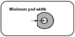
| Minimum pad width | For cut Lands,
specify the minimum pad width that is permitted, as illustrated
below. This is the distance from the outer edge of the drill hole
in the pad, to the outer edge of the pad. This is an optional
setting.
Note Annulus padstacks can be cut only if the following requirements are met. If either requirements is not met, then the annulus padstack is not cut and an error message is displayed.
For example, an annulus pad shape that has an outer diameter of 6.5mm and an internal diameter of 3.25mm cannot be cut using the Cut Land command. However, if it has an outer diameter of 6.5mm and an internal diameter of 3.24998mm then it can be cut. |
| Minimum number of thermal spokes | Specify the minimum number of thermal spokes that must come
in contact with a powerplane. This is an optional setting.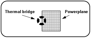 |