
Depending on the Mode and filter buttons, the following attributes can be displayed in the Attributes dialog. The Display label and Attribute label values are displayed for each attribute in the Attributes table. The Display label value is shown in the Customize Table Configuration Dialog and Constraint Browser dialogs for the relevant attribute. The Attribute label value provides a more detailed description of the attribute. To display the attributes for a particular mode and attribute type, click the relevant link below.
Mode: Signal
Attribute type:  Differential Pair
| Display label | Attribute label | Description | Associated Attribute Types |
|---|---|---|---|
| Clearance Class | Clearance Class | For the signals that you select in the Signals tree, this attribute allows you to specify a clearance class that you create in the Clearance Class Manager dialog. This dialog allows you to create clearance classes, and specify the design rule stack referred to between nets in each one. | Differential pair class, E-Net class, Net class, Differential pair, E-Net, Net. |
| Color | Color | For a selected signal, this attribute allows you to specify a color in the displayed Select color dialog. All items with the selected signal are displayed in the color that you specify. | Differential pair class, E-Net class, Net class, Component, Differential pair, E-Net, Net. |
| Coupled Length | Coupled Length | For the differential pair, the total length of routes is displayed that meet the track spacing requirements for differential pairs. These requirements are set in the Track spacing column in the Rule Editor Dialog: Differential Pairs Tab. This attribute is not available in Constraint Browser for eCADSTAR Schematic Editor. | Differential pair. |
| Coupled Ratio (%) | Coupled Ratio (%) | For the total length of routes in a differential pair, the percentage is displayed which meet the track spacing requirements for differential pairs. These requirements are set in the Track spacing column in the Rule Editor Dialog: Differential Pairs Tab. This attribute is not available in Constraint Browser for eCADSTAR Schematic Editor. | Differential pair. |
| Max. (Ω) | Differential Impedance Max. (Ω) | Allows you to specify the maximum differential impedance value that is permitted for the differential pair. | Differential pair class, Differential Pair, Pin Pair. |
| Min. (Ω) | Differential Impedance Min. (Ω) | Allows you to specify the minimum differential impedance value that is permitted for the differential pair. | Differential pair class, Differential Pair, Pin Pair. |
| Violated Length | Differential Impedance Violated Length | For the differential pair routes, the total length is displayed that violates the differential impedance value in the design. If values are entered for Min (Ω) and Max (Ω), then the Violated Length value for the relevant design is displayed when you click Update values in Constraint Browser. This attribute is not available in Constraint Browser for eCADSTAR Schematic Editor. | Differential Pair, E-Net, Net, Pin Pair. |
| Match Ratio (%) | Differential Impedance Match Ratio | For a differential pair, the percentage of the routes is displayed that does not violate the differential impedance value in the design. When you click Update values in Constraint Browser, differential impedance is calculated using the layer stack and material values in the design. The match ratio is not displayed if the minimum and maximum values of the differential impedance are not set. This attribute is not available in Constraint Browser for eCADSTAR Schematic Editor. | Differential Pair. |
| Differential Pair Class | Differential Pair Class | Using the Differential pair class dialog, specify a differential pair class that you create in the Differential Pair Class Manager dialog. | Differential Pair. |
| Differential Pair Rule Stack | Differential Pair Rule Stack | For a differential pair, this attribute allows you to specify
a differential pair rule stack from the Rule library. These are
created in the Rule
Editor Dialog: Differential Pairs Tab. Select a value in the
Rule Stack dialog. This dialog displayed by pointing the cursor in this cell, and then clicking the displayed
 button. button. |
Differential pair class, Differential Pair, Pin Pair. |
| Total Length | Differential Pair Total Length Actual | Allows you to display the total length of all routes in the differential pair when you click Update values in Constraint Browser. This attribute is not available in Constraint Browser for eCADSTAR Schematic Editor. | Differential Pair. |
| Hole/Area Design Rule Stack | Hole/Area Design Rule Stack | Allows you to specify a Hole/Area Design Rule Stack from the
Rule library, for the signals that you select in the Signals
tree. This defines the minimum clearances between holes and layout
areas, and conductor types. These are created in the Rule
Editor dialog, Conductor Clearance
tab, Hole/Area
sub tab. Select a value in the Rule
Stack dialog. This dialog displayed by pointing the cursor in
this cell, and then clicking the displayed
button. |
Differential pair class, E-Net class, Net class, Differential Pair, E-Net, Net. |
| Actual | Length Difference between Positive/Negative Actual | Allows you to display the maximum difference in length between the positive and negative tracks of a differential pair. Click Update values in Constraint Browser to display this value. If it is greater than the value specified in the Max. field (Length Difference between Positive/Negative Max.), then it is shown in red. This attribute is not available in Constraint Browser for eCADSTAR Schematic Editor. | Differential pair class, Differential Pair. |
| Max. | Length Difference between Positive/Negative Max. | Allows you to specify the maximum difference in length that is permitted between the positive and negative tracks of a differential pair. Specify a value that is greater than 0, and less than or equal to 20000mm. | Differential Pair. |
| Match Ratio for Differential Rule (%) | Match Ratio for Differential Rule (%) | For all routes in a selected differential pair, the percentage of their total length is displayed that does not violate the specified differential pair rule stack. This attribute is not available in Constraint Browser for eCADSTAR Schematic Editor. | Differential Pair. |
| Non-coupled Length | Non-coupled Length | For a differential pair, the total length of routes is displayed that do not meet the track spacing requirements for differential pairs. These requirements are set in the Track spacing column in the Rule Editor Dialog: Differential Pairs Tab. This attribute is not available in Constraint Browser for eCADSTAR Schematic Editor. | Differential Pair. |
| Max. | Pin Pair Delay Max. | This attribute allows you to specify the maximum propagation delay between the pins of the differential pair. | Differential pair class, E-Net class, Differential Pair, E-Net, Pin Pair, Skew Group. |
| Min. | Pin Pair Delay Min. | This attribute allows you to specify the minimum propagation delay between the pins of the differential pair. | Differential pair class, E-Net class, Differential Pair, E-Net, Pin Pair, Skew Group. |
| Max. | Pin Pair Length Max. | Allows you to specify the required maximum distance between the pin pairs. Specify a value that is greater than 0, and less than or equal to 20000mm. | Differential pair class, E-Net class, Net class, Differential Pair, E-Net, Net, Pin Pair, Skew Group. |
| Min. | Pin Pair Length Min. | Allows you to specify the required minimum distance between the pin pairs. Specify a value that is greater than 0, and less than or equal to 20000mm. | Differential pair class, E-Net class, Net class, E-Net, Net, Pin Pair, Skew Group. |
| Same Net Design Rule Stack | Same net Design Rule Stack | Allows you to specify a Same Net Design Rule Stack from the
Rule library. This defines the clearance that is applied, by default,
between conductors with the same net. These are created in the
Rule Editor dialog, Conductor
Clearance tab, Conductor
sub tab. Select a value in the Rule
Stack dialog. This dialog displayed by pointing the cursor in
this cell, and then clicking the displayed
button. |
Differential pair class, E-Net class, Net class, Differential Pair, E-Net, Net. |
| Signal | Signal | Allows you to display the signal that is associated with the item that you select. | Differential pair class, E-Net class, Net class, Differential Pair, E-Net, Net. Pin Pair. |
| Topology Template | Topology Template | Allows you to assign a compatible topology template to the
E-Net or differential pair that you select in the Signals
tree. This can be done using the Assign
Topology Template dialog, or by specifying its name in
the Topology Template cell.
This attribute is only available in a High Speed environment. Click
in this cell to display the Assign
Topology Template dialog.
You can also copy and paste an existing value
in this cell. If you attempt to specify an incompatible value,
then a warning message is shown, and the value is not updated.
An incompatible value may have a topology structure which does
not match the selected E-Net or differential pair. For example,
it may comprise a different number of ICs or passive components.
When you enter a compatible topology template,
it is automatically checked. If the topological structure of the
relevant signal does not follow the assigned topology template,
then the value in this cell is shown in red. The topology template
is also checked whenever the following actions are performed.
When the topological structure of the signal matches the assigned topology template, the value in this cell is immediately shown in black. |
Differential Pair, E-Net. |
| Violated Length for Differential Rule | Violated Length for Differential Rule | For a selected differential pair, this attribute allows you to display the total length of routes that violate the specified differential pair rule stack. This is displayed when you click Update values in Constraint Browser. This attribute is not available in Constraint Browser for eCADSTAR Schematic Editor. | Differential Pair. |
| Violated Length | Width Violation Length Actual | Allows you to display the length of track whose width is outside the values defined in the specified track width stack. This is selected in the Track Width Stack cell. Click Update values in Constraint Browser to display the Violated Length value. This attribute is not available in Constraint Browser for eCADSTAR Schematic Editor. | Differential Pair, E-Net, Net. Pin Pair. |
Attribute type:  E-Net
E-Net
| Display label | Attribute label | Description | Associated Attribute Types |
|---|---|---|---|
| Max. (Ω) | Characteristic Impedance Max. (Ω) | Allows you to specify the maximum characteristic impedance for the E-Net or net that you select in the Signals tree in Constraint Browser. | E-Net class, Net class, E-Net, Pin Pair. |
| Min. (Ω) | Characteristic Impedance Min. (Ω) | Allows you to specify the minimum characteristic impedance for the E-Net or net that you select in the Signals tree in Constraint Browser. | Net. |
| Clearance Class | Clearance Class | For the signals that you select in the Signals tree in Constraint Browser, this attribute allows you to specify a clearance class that you created in the Clearance Class Manager dialog. | E-Net class, Net class, Differential Pair, E-Net, Net. |
| Color | Color | For a selected signal, this attribute allows you to specify a color in the displayed Select color dialog. All items with the selected signal are displayed in the color that you specify. | E-Net class, Net class, Component, Differential Pair, E-Net, Net. |
| E-Net Class | E-Net Class | Allows you to specify an E-Net class that you created in the E-Net Class Manager dialog. Specify a value in the E-Net class dialog. | E-Net. |
| Edge Style | Edge Style | For a selected E-Net or E-Net class, this setting allows you to specify the angle of the segment end of the lengthen pattern. The value that you specify is used in preference to the value specified in the Design Settings dialog, Lengthen section. This attribute is not available in Constraint Browser for eCADSTAR Schematic Editor. | E-Net. |
| Hole/Area Design Rule Stack | Hole/Area Design Rule Stack | For the signals that you select in the Signals tree, specify a Hole/Area Design Rule Stack from the Rule library. This defines the minimum clearances between holes and layout areas, and conductor types. These are created in the Rule Editor dialog, Conductor Clearance tab, Hole/Area sub tab. | Differential pair class, E-Net class, Net class, Differential Pair, E-Net, Net. |
| Actual | Length Difference in Pin Pair Actual | Displays the maximum difference between the lengths in a Skew Group that is calculated when you click Update Values in Constraint Browser. If this value is greater than the Max. value that you specify, then it is shown in red. This attribute is not available in Constraint Browser for eCADSTAR Schematic Editor. | E-Net class, Net class, E-Net, Net, Skew Group. |
| Max. | Length Difference in Pin Pair Max. | Allows you to specify the maximum difference between the lengths of pin pairs in a selected Skew Group. | E-Net class, Net class, E-Net, Net, Skew Group. |
| Max. Size | Max. Size | For a selected E-Net or E-Net class, this attribute allows
you to set the maximum length applied between parallel routes when
lengthening a routing pattern. The value that you specify is used
in preference to the value specified in the Design
Settings dialog, Lengthen
section. This is illustrated below for the Accordion
meander mode.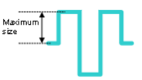 This attribute is not available in Constraint Browser for eCADSTAR Schematic Editor. |
E-Net. |
| Max. Via Count | Max. Via Count | Allows you to specify a maximum number of vias for a selected signal. If the calculated number of vias for the signal exceeds this value, then it is displayed in red in the Via Count cell. | E-Net class, Net class, E-Net, Net. |
| Meander Mode | Meander Mode | For a selected E-Net or E-Net class, this attribute allows you to specify the meander mode that is used to lengthen the E-Net. The value that you specify is used in preference to the value specified in the Design Settings dialog, Lengthen section. This attribute is not available in Constraint Browser for eCADSTAR Schematic Editor. | E-Net. |
| Min. Space | Min. Space | For a selected E-Net or E-Net class, this attribute allows
you to set the minimum space applied between parallel routes when
lengthening a routing pattern. The value that you specify is used
in preference to the value specified in the Design
Settings dialog, Lengthen
section. This is illustrated below for the Accordion
meander mode.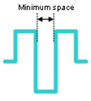 This attribute is not available in Constraint Browser for eCADSTAR Schematic Editor. |
E-Net. |
| Max. | Pin Pair Delay Max. | For the E-Net that you select in the Signals tree, this attribute allows you to specify the maximum delay that is permitted between the pin pairs. | Differential pair class, E-Net class, Differential Pair, E-Net, Pin Pair, Skew Group. |
| Min. | Pin Pair Delay Min. | For the E-Net that you select in the Signals tree, this attribute allows you to specify the minimum delay that is permitted between the pin pairs. | Differential pair class, E-Net class, Differential Pair, E-Net, Pin Pair, Skew Group. |
| Max. | Pin Pair Length Max. | For the E-Net, net or pin pair that you select in the Signals tree, this attribute allows you to specify the required maximum distance between the pin pairs. Specify a value that is greater than 0, and less than or equal to 20000mm. | Differential pair class, E-Net class, Net class, Differential Pair, E-Net, Net, Pin Pair, Skew Group. |
| Min. | Pin Pair Length Min. | For the E-Net, net or pin pair that you select in the Signals tree, specify the required minimum distance between the pin pairs. Specify a value that is greater than 0, and less than or equal to 20000mm. | Differential pair class, E-Net class, Net class, Differential Pair, E-Net, Net, Pin Pair, Skew Group. |
| Same Net Design Rule Stack | Same Net Design Rule Stack | For the signals that you select in the Signals
tree, this attribute allows you to specify a Same Net Design Rule
Stack from the Rule library. This defines the clearance that is
applied, by default, between conductors with the same net. These
are created in the Rule Editor
dialog, Conductor Clearance tab, Conductor sub tab.
Select a value in the Rule Stack
dialog. This dialog displayed by pointing the cursor in this cell,
and then clicking the displayed button. |
Differential pair class, E-Net class, Net class, Differential Pair, E-Net, Net. |
| Net name | Shield Net name | Using the Net selector dialog,
this attribute allows you to specify the signal name of the shield
pattern. You can narrow down the signals displayed in the dialog
by selecting or clearing the Ground,
Power and Signals
check boxes, and by filtering the displayed values using the Net name box. Note Shielding attributes are read-only for E-Nets in Constraint Browser for eCADSTAR PCB Editor. |
E-Net class, Net class, Net group, E-Net, Net. |
| Track Width Stack | Shield Track Width Stack | This attribute allows you to specify a Track Width Stack from
the Rule library. These are created in the Rule
Editor Dialog: Tracks Tab. Select a value in the Rule
Stack dialog. This dialog displayed by pointing the cursor in
this cell, and then clicking the displayed
button. |
E-Net class, Net class, E-Net, Net. |
| Gap | Shield Gap | Allows you to specify the clearance between the shield pattern and the track. | E-Net class, Net class, Net group, E-Net, Net. |
| Mode | Shield Mode | This attribute allows you to select from the following shield
pattern modes: OFF: shielding is not added around the relevant track. If shielding is set for an E-Net, this setting allows you to turn it off for a constituent net. Same Layer: shielding is added on the same layer around the track. Same/Adjacent Layers: shielding is added on the same layer and on adjacent layers around the track. Adjacent Layers: shielding is only added on adjacent layers around the track. |
E-Net class, Net class, Net group, E-Net, Net. |
| Signal | Signal | Allows you to display the signal that is associated with the items selected in the Signals tree in the Constraint Browser: Signals section, Signals Tab. | Differential pair class, E-Net class, Net class, Differential Pair, E-Net, Net, Pin Pair. |
| Topology Template | Topology Template | Allows you to assign a compatible topology template to the
E-Net or differential pair that you select in the Signals
tree. This can be done using the Assign
Topology Template dialog, or by specifying its name in
the Topology Template cell.
This attribute is only available in a High Speed environment. Click
in this cell to display the Assign
Topology Template dialog.
You can also copy and paste an existing value
in this cell. If you attempt to specify an incompatible value,
then a warning message is shown, and the value is not updated.
An incompatible value may have a topology structure which does
not match the selected E-Net or differential pair. For example,
it may comprise a different number of ICs or passive components.
When you enter a compatible topology template,
it is automatically checked. If the topological structure of the
relevant signal does not follow the assigned topology template,
then the value in this cell is shown in red. The topology template
is also checked whenever the following actions are performed.
When the topological structure of the signal matches the assigned topology template, the value in this cell is immediately shown in black. |
Differential Pair, E-Net. |
| Total Length | Total Length |
The total routing length is displayed for a selected E-Net or net. This is displayed when you click Update Values in the Constraint Browser: Signals section, Signals Tab. This attribute is not available in Constraint Browser for eCADSTAR Schematic Editor. |
E-Net, Net. |
| Max. | Total Length Max. | Allows you to specify a maximum value for the total length of all nets in a selected E-Net that is displayed in the Routing tab, Total Length column, in the Constraint Browser: Signals section, Signals Tab. If the value in the Total Length cell is greater than the value specified in the Total Length Max. cell, then it is displayed in red. | E-Net class, Net class, E-Net, Net. |
| Min. | Total Length Min. | Allows you to specify a minimum value for the total length of all nets in a selected E-Net that is displayed in the Routing tab, Total Length column, in the Constraint Browser: Signals section, Signals Tab. If the value in the Total Length cell is less than the value specified in the Total Length Min. cell, then it is displayed in red. | E-Net class, Net class, E-Net, Net. |
| Track Width Stack | Track Width Stack | For E-Nets and nets that you select in the Signals
tree, in the Constraint Browser:
Signals section, Signals Tab, this attribute allows you to
specify a Track Width Stack from the Rule library. These are created
in the Tracks tab in the Rule
Editor dialog. Select a value
in the Rule Stack dialog. This dialog displayed by pointing the cursor in this cell, and then clicking
the displayed button. |
E-Net class, Net class, E-Net, Net Pin Pair. |
| Unrouted Net Count | Unc. Count |
Displays the number of unrouted nets for a selected signal. This value is displayed in the Signals tab and Classes/Groups tab in Constraint Browser when you click Update Values. This attribute is not available in Constraint Browser for eCADSTAR Schematic Editor. |
Net. |
| Via Count | Via Count |
Displays the calculated number of vias for a selected item. If this exceeds the Max. Via Count value, then it is displayed in red. This attribute is not available in Constraint Browser for eCADSTAR Schematic Editor. |
E-Net class, Net class, E-Net, Net Pin Pair. |
| Voltage (V) | Voltage (V) | For E-Nets and nets, this attribute allows you to specify the voltage that is used for simulation purposes. | E-Net class, Net class, E-Net, Net. |
| Violated Length | Width Violation Length Actual |
For a selected E-Net or net, this attribute allows you to display the length of track whose width is outside the values defined in the specified track width stack. This is selected in the Track Width Stack cell. Click Update Values to display the Violated Length value. This attribute is not available in Constraint Browser for eCADSTAR Schematic Editor. |
Differential Pair, E-Net, Net, Pin Pair. |
Attribute
type:  Net
Net
| Display label | Attribute label | Description | Associated Attribute Types |
|---|---|---|---|
| Allow Ring | Allow Ring | Allows you to specify nets which are exempt from the Ring Removal function when manual
routing. Set Ring Removal to
ON in the Add
Route command to activate this function. This attribute is not available in Constraint Browser for eCADSTAR Schematic Editor. |
Net. |
| Max. (Ω) | Characteristic Impedance Max. (Ω) | For the E-Net, net or pin pair that you select in the Signals tree in the Signals tab and Classes/Groups tab in Constraint Browser, this attribute allows you to specify the required maximum distance between the pin pairs. Specify a value that is greater than 0, and less than or equal to 20000mm. | E-Net class, Net class, E-Net, Pin Pair. |
| Min. (Ω) | Characteristic Impedance Min. (Ω) | For the E-Net, net or pin pair that you select in the Signals tree in the Signals tab and Classes/Groups tab in Constraint Browser, this attribute allows you to specify the required minimum distance between the pin pairs. Specify a value that is greater than 0, and less than or equal to 20000mm. | E-Net class, Net class, E-Net, Pin Pair. |
| Clearance Class | Clearance Class | For the signals that you select in the Signals tree, this attribute allows you to specify a clearance class that you created in the Clearance Class Manager dialog. This dialog is displayed by clicking Utility > Clearance Class Manager in the Constraint Browser menu. | Differential pair class, E-Net class, Net class, Differential Pair, E-Net, Net. |
| Color | Color | For a selected signal, this attribute allows you to specify a color in the displayed Select color dialog. All items with the selected signal are displayed in the color that you specify. | Differential pair class, E-Net class, Net class, Component, Differential Pair, E-Net, Net. |
| Comment | Comment | Displays the comment that you associate with the selected item. | Component, Pin, Net. |
| Hole/Area Design Rule Stack | Hole/Area Design Rule Stack | For the signals that you select in the Signals
tree, this attribute allows you to specify a Hole/Area Design
Rule Stack from the Rule library. This defines the minimum clearances
between holes and layout areas, and conductor types. These are
created in the Rule Editor dialog,
Conductor Clearance tab, Hole/Area
sub tab. Select a value in the Rule
Stack dialog. This dialog displayed by pointing the cursor in
this cell, and then clicking the displayed
button.
Hole/Area Design Rule Stacks are defined in the
Rule Editor dialog, Conductor
Clearance tab, Hole/Area
sub tab. |
Differential pair class, E-Net class, Net class, Differential Pair, E-Net, Net. |
| Actual | Length Difference in Pin Pair Actual | The maximum difference between the lengths of two pins in a
pin pair that is calculated when you click Update
Values. If this value is greater than the Max.
value that you specify, then it is shown in red. This attribute is not available in Constraint Browser for eCADSTAR Schematic Editor. |
E-Net class, Net class, E-Net, Net, Skew Group. |
| Max. | Length Difference in Pin Pair Max. | Allows you to specify the maximum difference between the lengths
of two pins in a pin pair. This attribute is not available in Constraint Browser for eCADSTAR Schematic Editor. |
E-Net class, Net class, E-Net, Net, Skew Group. |
| Max. Via Count | Max. Via Count | Allows you to specify a maximum number of vias for a selected
item. This attribute is only available in a High Speed environment.
You can specify a value for the following items:
|
E-Net class, Net class, E-Net, Net. |
| Net Class | Net Class | Using the Net class dialog, this attribute allows you to specify a net class that you created in the Net Class Manager dialog. This is accessed by clicking Edit > Net Class Manager in the Constraint Browser dialog. | Net. |
| Net Layer | Net Layer | For a selected net, this attribute allows you to specify the
conductor layers on which it can be routed on using the Autorouter.
Select the required conductor layers in the displayed Net
Layer dialog. Display this dialog by pointing the cursor
at this cell and then clicking the button.
You can set a value for this column in the Routing
tab in either the Signals
tab or Classes/Groups
tab in Constraint Browser. The value is automatically set
in both locations when you enter it. This attribute is not available in Constraint Browser for eCADSTAR Schematic Editor. |
Net class, Net. |
| Net Type | Net Type | Allows you to set the net or bus to one of the following options:
This attribute is not available in Constraint Browser for eCADSTAR PCB Editor. |
Net. |
| No. of required Testpoints | No. of required Testpoints |
Shows the number of testpoints for a selected net, and allows you to specify a value. You can set a value for this column in the Routing tab in either the Signals tab or Classes/Groups tab in Constraint Browser. The value is automatically set in both locations when you enter it. This attribute is not available in Constraint Browser for eCADSTAR Schematic Editor. |
Net. |
| Max. | Pin Pair Length Max. | For the E-Net, net or pin pair that you select in the Signals tree, this attribute allows you to specify the required maximum distance between the pin pairs. Specify a value that is greater than 0, and less than or equal to 20000mm. | Differential pair class, E-Net class, Net class, Differential Pair, E-Net, Net, Pin Pair, Skew Group. |
| Min. | Pin Pair Length Min. | For the E-Net, net or pin pair that you select in the Signals tree, specify the required minimum distance between the pin pairs. Specify a value that is greater than 0, and less than or equal to 20000mm. | Differential pair class, E-Net class, Net class, Differential Pair, E-Net, Net, Pin Pair, Skew Group. |
| Same Net Design Rule Stack | Same Net Design Rule Stack | Allows you to specify a Same Net Design Rule Stack from the
Rule library. This defines the clearance that is applied, by default,
between conductors with the same net. These are created in the
Rule Editor dialog, Conductor
Clearance tab, Conductor
sub tab. Select a value in the Rule
Stack dialog. This dialog displayed by pointing the cursor in
this cell, and then clicking the displayed
button.
Same Net Design Rule Stacks are defined in the Rule
Editor dialog, Conductor Clearance
tab, Conductor
sub tab. |
Differential pair class, E-Net class, Net class, Differential Pair, E-Net, Net. |
| Net name | Shield Net name | Using the Net selector dialog, this attribute allows you to specify the signal name of the shield pattern. You can narrow down the signals displayed in the dialog by selecting or clearing the GND, Power and Signals check boxes, and by filtering the displayed values using the Net name box. | E-Net class, Net class, Net group, E-Net, Net. |
| Track Width Stack | Shield Track Width Stack | This attribute allows you to specify a Track Width Stack from
the Rule library. These are created in the Rule
Editor Dialog: Tracks Tab. Select a value in the Rule
Stack dialog. This dialog displayed by pointing the cursor in
this cell, and then clicking the displayed
button. |
E-Net class, Net class, E-Net, Net. |
| Gap | Shield Gap | Allows you to specify the clearance between the shield pattern and the track. | E-Net class, Net class, Net group, E-Net, Net. |
| Mode | Shield Mode | This attribute allows you to select from the following shield
pattern modes: OFF: shielding is not added around the relevant track. If shielding is set for an E-Net, this setting allows you to turn it off for a constituent net. Same Layer: shielding is added on the same layer around the track. Same/Adjacent Layers: shielding is added on the same layer and on adjacent layers around the track. Adjacent Layers: shielding is only added on adjacent layers around the track. |
E-Net class, Net class, Net group, E-Net, Net. |
| Signal | Signal | Allows you to display the signal that is associated with the item that you select. | Differential pair class, E-Net class, Net class, Differential Pair, E-Net, Net, Pin Pair. |
| Total Length | Total Length |
The total routing length is displayed for a selected E-Net or net. This is displayed when you click Update Values in the Constraint Browser: Signals section, Signals Tab. This attribute is not available in Constraint Browser for eCADSTAR Schematic Editor. |
E-Net, Net. |
| Max. | Total Length Max. | Allows you to specify a maximum value for the total length of all nets in a selected E-Net that is displayed in the Routing tab, Total Length column, in the Constraint Browser: Signals section, Signals Tab. If the value in the Total Length cell is greater than the value specified in the Total Length Max. cell, then it is displayed in red. | E-Net class, Net class, E-Net, Net. |
| Min. | Total Length Min. | Allows you to specify a minimum value for the total length of all nets in a selected E-Net that is displayed in the Routing tab, Total Length column, in the Constraint Browser: Signals section, Signals Tab. If the value in the Total Length cell is less than the value specified in the Total Length Min. cell, then it is displayed in red. | E-Net class, Net class, E-Net, Net. |
| Track width Stack | Track width Stack | For E-Nets and nets that you select in the Signals
tree, in the Constraint Browser:
Signals section, Signals Tab, this attribute allows you to
specify a Track Width Stack from the Rule library. These are created
in the Tracks tab in the Rule
Editor dialog. Select a value
in the Rule Stack dialog. This dialog displayed by pointing the cursor in this cell, and then clicking
the displayed button. |
E-Net class, Net class, E-Net, Net, Pin Pair. |
| Unrouted Net Count | Unc. Count | Displays the number of unrouted nets for a selected signal.
This value is displayed in the Signals
tab and Classes/Groups
tab in Constraint Browser when you click Update
Values. This attribute is not available in Constraint Browser for eCADSTAR Schematic Editor. |
Net. |
| Via Count | Via Count | Displays the calculated number of vias for a selected item.
If this exceeds the Max.
Via Count value, then it is displayed in red. This attribute is not available in Constraint Browser for eCADSTAR Schematic Editor. |
E-Net class, Net class, E-Net, Net, Pin Pair. |
| Voltage (V) | Voltage (V) | Specify the voltage that is used for simulation purposes. You can specify a value for E-Nets, E-Net classes, nets and net classes. The value is displayed in Voltage column in the Signals tab and Classes/Groups tab in Constraint Browser. | E-Net class, Net class, E-Net, Net. |
| Violated Length | Width Violation Length Actual | Allows you to display the length of track whose width is outside
the values defined in the specified track width stack. This is
selected in the Track Width Stack
cell. Click Update values in
Constraint
Browser to display the Violated
Length value. This attribute is not available in Constraint Browser for eCADSTAR Schematic Editor. |
Differential Pair, E-Net, Net, Pin Pair. |
Attribute type:  Component
| Display label | Attribute label | Description | Associated Attribute Types |
|---|---|---|---|
| 0 | 0 | For a selected component, this attribute allows you to specify a permitted placement angle of 0 degrees. This attribute is not available in Constraint Browser for eCADSTAR Schematic Editor. | Component. |
| 45 | 45 | For a selected component, this attribute allows you to specify a permitted placement angle of 45 degrees. This attribute is not available in Constraint Browser for eCADSTAR Schematic Editor. | Component. |
| 90 | 90 | For a selected component, this attribute allows you to specify a permitted placement angle of 90 degrees. This attribute is not available in Constraint Browser for eCADSTAR Schematic Editor. | Component. |
| 135 | 135 | For a selected component, this attribute allows you to specify a permitted placement angle of 135 degrees. This attribute is not available in Constraint Browser for eCADSTAR Schematic Editor. | Component. |
| 180 | 180 | For a selected component, this attribute allows you to specify a permitted placement angle of 180 degrees. This attribute is not available in Constraint Browser for eCADSTAR Schematic Editor. | Component. |
| 225 | 225 | For a selected component, this attribute allows you to specify a permitted placement angle of 225 degrees. This attribute is not available in Constraint Browser for eCADSTAR Schematic Editor. | Component. |
| 270 | 270 | For a selected component, this attribute allows you to specify a permitted placement angle of 270 degrees. This attribute is not available in Constraint Browser for eCADSTAR Schematic Editor. | Component. |
| 315 | 315 | For a selected component, this attribute allows you to specify a permitted placement angle of 315 degrees. This attribute is not available in Constraint Browser for eCADSTAR Schematic Editor. | Component. |
| Color | Color | Allows you to specify the display color of the component area
that is associated with the component selected in the Components
tree. Specify a color in the Select color
dialog and click OK. This dialog
is displayed by pointing the cursor at the Color
cell, and then clicking the displayed
button. In 3D View mode, the
component is displayed in the color that you specify. This attribute
is not available in Constraint
Browser for eCADSTAR Schematic Editor. |
Differential pair class, E-Net class, Net class, Component, Differential Pair, E-Net, Net. |
| Comment | Comment | Displays the comment that you associate with the selected item. | Component, Pin, Net. |
| Current Rating | Current Rating | The nominal current rating that is specified for a component. | Component. |
| Device Type | Device Type | Displays whether the part associated with a selected component is either active or passive. This attribute is not available in Constraint Browser for eCADSTAR Schematic Editor. | Component. |
| Dimensions | Dimensions | Displays the dimensions of the component that are specified in the Library Editor Panel: Parts tab, or the Part Editor Panel: Properties tab, Dimensions column. | Component. |
| Frequency | Frequency | Displays the frequency of the component that is specified in the Library Editor Panel: Parts tab, or the Part Editor Panel: Properties tab, Frequency column. | E-Net class, Net class, E-Net, Net. |
| Gender | Gender | Displays the gender of the component that is specified in the Library Editor Panel: Parts tab, or the Part Editor Panel: Properties tab, Gender column. The gender of a component can be specified as "male" (plug) or "female" (socket). | Component. |
| Manufacturer | Manufacturer | Displays the Manufacturer for the component that is specified in the Library Editor Panel: Parts tab, or the Part Editor Panel: Properties tab, Manufacturer column. | Component. |
| Manufacturer Part Number | Manufacturer Part Number | Displays the Manufacturer Part Number for the component that is specified in the Library Editor Panel: Parts tab, or the Part Editor Panel: Properties tab, Manufacturer Part Number column. | Component. |
| Maximum Height | Maximum Height | For a selected part, this attribute allows you to display the distance between the top of the part and the board. This is specified in the Maximum Height (mm) column, in the Library Editor Panel: Parts tab. The value must be greater than the Standoff Height value. This attribute is not available in Constraint Browser for eCADSTAR Schematic Editor. | Component. |
| Maximum Operating Temperature | Maximum Operating Temperature | Displays the maximum operating temperature of the component that is specified in the Library Editor Panel: Parts tab, or the Part Editor Panel: Properties tab, Maximum Operating Temperature column. | Component. |
| Minimum Operating Temperature | Minimum Operating Temperature | Displays the minimum operating temperature of the component that is specified in the Library Editor Panel: Parts tab, or the Part Editor Panel: Properties tab, Minimum Operating Temperature column. | Component. |
| Mounting Type | Mounting Type | Displays the mounting type that is specified in the Library Editor Panel: Parts tab, or the Part Editor Panel: Properties tab, Mounting Type column. Mounting types for a component might include "through-hole" or "surface mount". | Component. |
| Number of Rows | Number of Rows | Displays the number of rows of pins on the component that is specified in the Library Editor Panel: Parts tab, or the Part Editor Panel: Properties tab, Number of Rows column. | Component. |
| Package Type | Package Type | Displays the type of package for the component that is specified in the Library Editor Panel: Parts tab, or the Part Editor Panel: Properties tab, Package Type column. A package type has a defined set of physical dimensions that the component has to conform to. Typically, the pitch spacing, height and general shape of the component is defined. for each package. | Component. |
| Part | Part | Displays the part name associated with the relevant component. | Component. |
| Part Number | Part Number | Displays the part number of the component that is specified in the Library Editor Panel: Parts tab, or the Part Editor Panel: Properties tab, Part Number column. | Component. |
| Passive Type | Passive Type | Displays the type of passive component. These are specified
in the Library
Editor Panel: Parts tab, or the Part
Editor Panel: Properties tab, Passive
Type column. The following values may be displayed.
|
Component. |
| Permitted Placement Side | Permitted Placement Side | For a selected component, this attribute allows you to specify its permitted placement side. This attribute is not available in Constraint Browser for eCADSTAR Schematic Editor. | Component. |
| Pin Count | Pin Count | The number of pins is displayed for a selected part. | Component. |
| Placement Group Name | Placement Group Name | Allows you to specify a placement group. See Placing Proximity Components. | Component, Pin. |
| Standoff Height | Standoff Height | For a selected part, the distance is displayed between the bottom of the part and the board. This is specified in the Standoff Height (mm) column, in the Library Editor Panel: Parts tab. This attribute is not available in Constraint Browser foreCADSTAR Schematic Editor. | Component. |
| Terminal Pitch | Terminal Pitch | Displays the distance between the pins on the component that are specified in the Library Editor Panel: Parts tab, or the Part Editor Panel: Properties tab, Terminal Pitch column. | Component. |
| Tolerance | Tolerance | Displays the tolerance for the Value attribute. This is specified in the Library Editor Panel: Parts tab, or the Part Editor Panel: Properties tab, Tolerance column. | Component. |
| Value | Value | Displays the value associated with the selected item. | Component. |
| Vendor Name | Vendor Name | Displays the Vendor Name that is associated with the component. This is specified in the Library Editor Panel: Parts tab, or the Part Editor Panel: Properties tab, Vendor Name column. | Component. |
| Vendor Reference | Vendor Reference | Displays the Vendor Reference that is associated with the component. This is specified in the Library Editor Panel: Parts tab, or the Part Editor Panel: Properties tab, Vendor Reference column. | Component. |
| Voltage Rating | Voltage Rating | Displays the voltage rating of the component. This is specified in the Library Editor Panel: Parts tab, or the Part Editor Panel: Properties tab, Voltage Rating column. | Component. |
| Wattage | Wattage | Displays the electrical power of the component, expressed in watts. This is specified in the Library Editor Panel: Parts tab, or the Part Editor Panel: Properties tab, Wattage column. | Component. |
Attribute type:  Pin
Pin
| Display label | Attribute label | Description | Associated Attribute Types | ||||||||||||||||||||||||||||
|---|---|---|---|---|---|---|---|---|---|---|---|---|---|---|---|---|---|---|---|---|---|---|---|---|---|---|---|---|---|---|---|
| Model Name | Model Name | Displays the pin buffer model that is assigned to the relevant
pin. This value is added when you create a new PCB design. It
is also added to the Analysis tab
in the Constraint
Browser: Component/Parts Section, Components Tab.
To ensure that the displayed information is current,
perform a Simulation Library Reload.
This is required if you:
Note If there are any failed pin assignments, these are listed when you execute the Simulation Library Reload command after selecting a model for the first time. |
Pin. | ||||||||||||||||||||||||||||
| Model Type | Model Type | Displays the type of pin buffer model that is assigned to the
relevant pin. The following types are supported in eCADSTAR.
Note If there are any failed pin assignments, these are listed when you execute the Simulation Library Reload command after selecting a model for the first time. |
Pin. | ||||||||||||||||||||||||||||
| Net | Net | Displays the net that is associated with the selected item. | Pin. | ||||||||||||||||||||||||||||
| Pin Circuit Label | Pin Circuit Label | When implied power is specified for a part in eCADSTAR Library Editor, the embedded signal is displayed that is associated with the relevant pin. This attribute is not available in Constraint Browser for eCADSTAR PCB Editor. | Pin. | ||||||||||||||||||||||||||||
| Pin Name | Pin Name | Displays the names of the pins that are associated with a signal. These are defined in the Part Editor in eCADSTAR Library Editor. | Pin. | ||||||||||||||||||||||||||||
| Pin Number | Pin Number | Displays the pin number for a selected pin. This is defined in the Part Editor in eCADSTAR Library Editor. | Pin. | ||||||||||||||||||||||||||||
| Pin Type | Pin Type | Displays the pin type of the selected item. This attribute is
not available in Constraint
Browser for eCADSTAR Schematic Editor.
The following values may be displayed.
|
Pin. | ||||||||||||||||||||||||||||
| Placement Group Name | Placement Group Name | Allows you to specify a placement group. See Placing Proximity Components. | Component, Pin. | ||||||||||||||||||||||||||||
| Signal | Signal | Displays the signal is that is associated with the selected pin. | Differential pair class, E-Net class, Net-class, Differential Pair, E-Net, Net, Pin Pair. |
 INPUT
INPUT OUTPUT
 BIDIRECT
 POWER
POWER GROUND
 NC
NCAttribute type:
 Pin
Pair
Pin
Pair
| Display label | Attribute label | Description | Associated Attribute Types |
|---|---|---|---|
| Match Ratio (%) | Characteristic Impedance Match Ratio | For the total length of the E-Net or net that you select in the Signals tree, the percentage is displayed which is within the minimum and maximum impedance values that you specify. When you click Update values, characteristic impedance is calculated using the layer stack and material values in the design. The match ratio is not displayed if the minimum and maximum values of the characteristic impedance are not set. This attribute is not available in Constraint Browser for eCADSTAR Schematic Editor. | Pin Pair. |
| Max. (Ω) | Characteristic Impedance Max. (Ω) | For the E-Net or net that you select in the Signals tree, specify the maximum characteristic impedance. This attribute is not available in Constraint Browser for eCADSTAR Schematic Editor. | E-Net class, Net-class, E-Net, Pin Pair. |
| Min. (Ω) | Characteristic Impedance Min. (Ω) | For the E-Net or net that you select in the Signals tree, specify the minimum characteristic impedance. This attribute is not available in Constraint Browser for eCADSTAR Schematic Editor. | E-Net class, Net-class, E-Net, Pin Pair. |
| Max. (Ω) | Differential Impedance Max. (Ω) | Specify the maximum differential impedance value that is permitted for the differential pair. | Differential pair class, Differential Pair, Pin Pair. |
| Min. (Ω) | Differential Impedance Min. (Ω) | Specify the minimum differential impedance value that is permitted for the differential pair. | Differential pair class, Differential Pair, Pin Pair. |
| Differential Pair Rule Stack | Differential Pair Rule Stack | For a differential pair, specify a differential pair rule stack
from the Rule library. These are created in the Rule
Editor Dialog: Differential Pairs Tab. Select a value in the
Rule Stack dialog. This dialog displayed by pointing the cursor in this cell, and then clicking the displayed
button. |
Differential pair class, Differential Pair. |
| Actual | Length Difference between Positive/Negative Actual | This attribute shows the maximum difference in length between the positive and negative tracks of a differential pair. This is displayed when you click Update values in Constraint Browser. This attribute is not available in Constraint Browser for eCADSTAR Schematic Editor. | Differential pair class, Differential Pair. |
| Actual | Pin Pair Delay Actual | For a pin pair that you select in the Signals tree, the calculated propagation delay is displayed when you click Update values in Constraint Browser. This value is calculated based on the pin pair lengths in the design. This attribute is not available in Constraint Browser for eCADSTAR Schematic Editor. See Creating Multiple Pin Pairs. | Pin Pair. |
| Max. | Pin Pair Delay Max. | For the E-Net that you select in the Signals tree, specify the maximum delay that is permitted between the pin pairs. | Differential pair class, E-Net class, Differential Pair, E-Net, Pin Pair, Skew Group. |
| Min. | Pin Pair Delay Min. | For the E-Net that you select in the Signals tree, specify the minimum delay that is permitted between the pin pairs. | Differential pair class, E-Net class, Differential Pair, E-Net, Pin Pair, Skew Group. |
| Actual | Pin Pair Length Actual. | If you select a pin pair in the Signals
tree, then its length in the design is displayed when you click Update values in Constraint
Browser. If the displayed value is outside of the minimum
or maximum values that you specify for the relevant E-Net, net
or pin pair, then it is displayed in red. See Creating
Multiple Pin Pairs. This attribute is not available in Constraint
Browser for eCADSTAR Schematic Editor.
Note The actual routed length of the pin pair is shown, rather than the manhattan length. |
Pin Pair. |
| Max. | Pin Pair Length Max. | For the E-Net, net or pin pair that you select in the Signals tree, this attribute allows you to specify the required maximum distance between the pin pairs. Specify a value that is greater than 0, and less than or equal to 20000mm. | Differential pair class, E-Net class, Net class, Differential Pair, E-Net, Net, Pin Pair, Skew Group. |
| Pin Pair Length Max. Actual | Pin Pair Length Max. Actual | This attribute is not available in Constraint Browser for eCADSTAR Schematic Editor. | Differential pair class, E-Net class, Net class, Differential Pair, E-Net, Net, Pin Pair, Skew Group. |
| Min. | Pin Pair Length Min. | For the E-Net, net or pin pair that you select in the Signals tree, this attribute allows you to specify the required minimum distance between the pin pairs. Specify a value that is greater than 0, and less than or equal to 20000mm. | Differential pair class, E-Net class, Net class, E-Net, Net, Pin Pair, Skew Group. |
| Pin Pair Length Min. Actual | Pin Pair Length Min. Actual | This attribute is not available in Constraint Browser for eCADSTAR Schematic Editor. | Differential pair class, E-Net class, Net class, Differential Pair, E-Net, Net, Pin Pair, Skew Group. |
| Track Width Stack | Track Width Stack | For E-Nets and nets that you select in the Signals
tree, this attribute allows you to specify a Track Width Stack
from the Rule library. These are created in the Tracks
tab in the Rule Editor dialog. In Constraint
Browser for eCADSTAR PCB Editor,
select a value in the displayed Track
Width Stack dialog. This attribute is not available in Constraint
Browser for
eCADSTAR Schematic Editor.
Note
|
E-Net class, Net class, E-Net, Net, Pin Pair. |
| Via Count | Via Count | Displays the calculated number of vias for a selected item. If this exceeds the Max. Via Count value, then it is displayed in red. This attribute is not available in Constraint Browser for eCADSTAR Schematic Editor. | E-Net class, Net class, E-Net, Net, Pin Pair. |
| Violated Length | Width Violation Length Actual | Allows you to display the length of track whose width is outside the values defined in the specified track width stack. This is selected in the Track Width Stack cell. Click Update values in Constraint Browser to display the Violated Length value. This attribute is not available in Constraint Browser for eCADSTAR Schematic Editor. | Differential Pair, E-Net, Net, Pin Pair. |
Mode: Class/Group
Attribute type:  Net class
See: Net.
Attribute type:  E-Net class
See: E-Net.
Attribute type:  Differential
pair class
Differential
pair class
See: Differential Pair.
Attribute type:  Net
group
Net
group
| Display label | Attribute label | Description | Associated Attribute Types |
|---|---|---|---|
| Net name | Shield Net name | Using the Net selector dialog, this attribute allows you to specify the signal name of the shield pattern. You can narrow down the signals displayed in the dialog by selecting or clearing the Ground, Power and Signals check boxes, and by filtering the displayed values using the Net name box. | E-Net class, Net class, Net group, E-Net, Net. |
| Gap | Shield Gap | Allows you to specify the clearance between the shield pattern and the track. | E-Net class, Net class, Net group, E-Net, Net. |
| Mode | Shield Mode | This attribute allows you to select from the following shield
pattern modes: OFF: shielding is not added around the relevant track. If shielding is set for an E-Net, this setting allows you to turn it off for a constituent net. Same Layer: shielding is added on the same layer around the track. Same/Adjacent Layers: shielding is added on the same layer and on adjacent layers around the track. Adjacent Layers: shielding is only added on adjacent layers around the track. |
E-Net class, Net class, Net group, E-Net, Net. |
Attribute type: Differential Pair
See: Differential Pair.
Attribute type: E-Net
See: E-Net.
Attribute type:
Net
See: Net.
Mode: Skew Group
Attribute type:  Skew Group
| Display label | Attribute label | Description | Associated Attribute Types |
|---|---|---|---|
| Actual | Delay Difference in Pin Pair Actual | The calculated maximum propagation time between two pins in a pin pair. This value is displayed in Constraint Browser for eCADSTAR PCB Editor when you click Update values in Constraint Browser. This attribute is not available in Constraint Browser for eCADSTAR Schematic Editor. | Skew Group. |
| Actual | Length Difference in Pin Pair Actual. | Displays the maximum difference between the lengths in a Skew Group that is calculated when you click Update values in Constraint Browser. If this value is greater than the Max. value that you specify, then it is shown in red. This attribute is not available in Constraint Browser for eCADSTAR Schematic Editor. | E-Net class, Net class, E-Net, Net, Skew Group. |
| Max. | Length Difference in Pin Pair Max. | Allows you to specify the maximum difference between the lengths of pin pairs in a selected Skew Group. | E-Net class, Net class, E-Net, Net, Skew Group. |
| Max. | Pin Pair Delay Max. | For the E-Net that you select in the Signals tree, this attribute allows you to specify the maximum delay that is permitted between the pin pairs. | Differential pair class, E-Net class, Differential Pair, E-Net, Pin Pair, Skew Group. |
| Min. | Pin Pair Delay Min. | For the E-Net that you select in the Signals tree, this attribute allows you to specify the minimum delay that is permitted between the pin pairs. | Differential pair class, E-Net class, Differential Pair, E-Net, Pin Pair, Skew Group. |
| Max. | Pin Pair Length Max. | For the E-Net, net or pin pair that you select in the Signals tree, this attribute allows you to specify the required maximum distance between the pin pairs. Specify a value that is greater than 0, and less than or equal to 20000mm. | Differential pair class, E-Net class, Net class, Differential Pair, E-Net, Net, Pin Pair, Skew Group. |
| Min. | Pin Pair Length Min. | For the E-Net, net or pin pair that you select in the Signals tree, specify the required minimum distance between the pin pairs. Specify a value that is greater than 0, and less than or equal to 20000mm. | Differential pair class, E-Net class, Net class, E-Net, Net, Pin Pair, Skew Group. |
| Max. | Relative Delay Difference Max. | For a selected Skew Group, specify the maximum propagation time for the Skew Group, relative to the specified base signal. | Skew Group. |
| Actual | Relative Delay Difference Max. Actual | The calculated maximum propagation time for the Skew Group, relative to the specified base signal. This value is displayed in Constraint Browser for eCADSTAR PCB Editor when you click Update values in Constraint Browser. This attribute is not available in Constraint Browser for eCADSTAR Schematic Editor. | Skew Group. |
| Min. | Relative Delay Difference Min. | For a selected Skew Group, specify the minimum propagation time for the Skew Group, relative to the specified base signal. | Skew Group. |
| Actual | Relative Delay Difference Min. Actual | The calculated minimum propagation time for the Skew Group, relative to the specified base signal. This value is displayed in Constraint Browser for eCADSTAR PCB Editor when you click Update values in Constraint Browser. This attribute is not available in Constraint Browser for eCADSTAR Schematic Editor. | Skew Group. |
| Max. | Relative Length Difference Max. | For a selected Skew Group, specify the maximum difference between the lengths in the Skew Group and the length of the base signal. | Skew Group. |
| Actual | Relative Length Difference Max. Actual | The calculated maximum difference between the lengths in the Skew Group and the length of the base signal. This value is displayed in Constraint Browser for eCADSTAR PCB Editor when you click Update values in Constraint Browser. This attribute is not available in Constraint Browser for eCADSTAR Schematic Editor. | Skew Group. |
| Min. | Relative Length Difference Min. | For a selected Skew Group, specify the minimum difference between the lengths in the Skew Group and the length of the base signal. | Skew Group. |
| Actual | Relative Length Difference Min. Actual | The calculated minimum difference between the lengths in the Skew Group and the length of the base signal. This value is displayed in Constraint Browser for eCADSTAR PCB Editor when you click Update values in Constraint Browser. This attribute is not available in Constraint Browser for eCADSTAR Schematic Editor. | Skew Group. |
Attribute type:  Pin Pair
See: Pin pair.
Mode: Component
This mode is not available in Constraint Browser for eCADSTAR Schematic Editor.
Attribute type: Component
See: Component.
Attribute type: Pin
See: Pin.
Mode: Part
This mode is not available in Constraint Browser for eCADSTAR Schematic Editor.
Attribute type: Part
The following attributes that are displayed are read-only.
| Display label | Attribute label | Description | Associated Attribute Types |
|---|---|---|---|
| 0 | 0 | For a selected part, this attribute allows you to specify a permitted placement angle of 0 degrees. | Component. |
| 45 | 45 | For a selected part, this attribute allows you to specify a permitted placement angle of 45 degrees. | Component. |
| 90 | 90 | For a selected part, this attribute allows you to specify a permitted placement angle of 90 degrees. | Component. |
| 135 | 135 | For a selected part, this attribute allows you to specify a permitted placement angle of 135 degrees. | Component. |
| 180 | 180 | For a selected part, this attribute allows you to specify a permitted placement angle of 180 degrees. | Component. |
| 225 | 225 | For a selected part, this attribute allows you to specify a permitted placement angle of 225 degrees. | Component. |
| 270 | 270 | For a selected part, this attribute allows you to specify a permitted placement angle of 270 degrees. | Component. |
| 315 | 315 | For a selected part, this attribute allows you to specify a permitted placement angle of 315 degrees. | Component. |
| Comment | Comment | Displays the comment that you associate with the selected item. | Component, Pin, Net. |
| Current Rating | Current Rating | The nominal current rating that is specified for a part. | Component. |
| Decap | Decoupling Capacitor | If selected, then the relevant part is specified as a decoupling capacitor (decap). The icon for the part in the Parts tree is updated to indicate that it is a decoupling capacitor. You can add decoupling capacitors to the library using theComponent Settings Dialog. In order to use them in a design, you must add them from the library. This is done by clickingImport Design Rule Library (Partial)orImport (Design Rule Library)in theRule Editor Dialog, in. Any two-pin device can be set as a | Component. |
| Device Type | Device Type | Displays whether the part associated with a selected component is either active or passive. | Component. |
| Dimensions | Dimensions | Displays the dimensions of the part that are specified in the Library Editor Panel: Parts tab, or the Part Editor Panel: Properties tab, Dimensions column. | Component. |
| Frequency | Frequency | Displays the frequency of the part that is specified in the Library Editor Panel: Parts tab, or the Part Editor Panel: Properties tab, Frequency column. | E-Net class, Net class, E-Net, Net. |
| Gender | Gender | Displays the gender of the part that is specified in the Library Editor Panel: Parts tab, or the Part Editor Panel: Properties tab, Gender column. The gender of a part can be specified as "male" (plug) or "female" (socket). | Component. |
| Jumper | Jumper | If selected, then the relevant part is specified as a jumper. The icon for the part in the Parts tree is updated to indicate that it is a jumper. You can add a jumper to the library using the Component Settings Dialog. You must then set it as jumper in the Part Editor Panel: Detail Tab, Part Information section. In order to use them in a design, you must add them from the library. This is done by clicking Import Design Rule Library (Partial) or Import (Design Rule Library) in the Rule Editor Dialog, in eCADSTAR PCB Editor. | Component. |
| Manufacturer | Manufacturer | Displays the Manufacturer for the part that is specified in the Library Editor Panel: Parts tab, or the Part Editor Panel: Properties tab, Manufacturer column. | Component. |
| Manufacturer Part Number | Manufacturer Part Number | Displays the Manufacturer Part Number for the part that is specified in the Library Editor Panel: Parts tab, or the Part Editor Panel: Properties tab, Manufacturer Part Number column. | Component. |
| Maximum Height | Maximum Height | For a selected part, this attribute allows you to display the distance between the top of the part and the board. This is specified in the Maximum Height (mm) column, in the Library Editor Panel: Parts tab. The value must be greater than the Standoff Height value. | Component. |
| Maximum Operating Temperature | Maximum Operating Temperature | Displays the maximum operating temperature of the part that is specified in the Library Editor Panel: Parts tab, or the Part Editor Panel: Properties tab, Maximum Operating Temperature column. | Component. |
| Minimum Operating Temperature | Minimum Operating Temperature | Displays the minimum operating temperature of the part that is specified in the Library Editor Panel: Parts tab, or the Part Editor Panel: Properties tab, Minimum Operating Temperature column. | Component. |
| Mounting Type | Mounting Type | Displays the mounting type that is specified in the Library Editor Panel: Parts tab, or the Part Editor Panel: Properties tab, Mounting Type column. Mounting types for a part might include "through-hole" or "surface mount". | Component. |
| Number of Rows | Number of Rows | Displays the number of rows of pins on the part that is specified in the Library Editor Panel: Parts tab, or the Part Editor Panel: Properties tab, Number of Rows column. | Component. |
| Package Type | Package Type | Displays the type of package for the part that is specified in the Library Editor Panel: Parts tab, or the Part Editor Panel: Properties tab, Package Type column. A package type has a defined set of physical dimensions that the component has to conform to. Typically, the pitch spacing, height and general shape of the component is defined. for each package. | Component. |
| Part Number | Part Number | Displays the part number of the part that is specified in the Library Editor Panel: Parts tab, or the Part Editor Panel: Properties tab, Part Number column. | Component. |
| Passive Type | Passive Type | Displays the type of passive component. These are specified
in the Library
Editor Panel: Parts tab, or the Part
Editor Panel: Properties tab, Passive
Type column. The following values may be displayed.
|
Component. |
| Permitted Placement Side | Permitted Placement Side | For a selected part , this attribute allows you to specify its permitted placement side. | Component. |
| Pin Count | Pin Count | The number of pins is displayed for a selected part. | Component. |
| Standoff Height | Standoff Height | For a selected part, the distance is displayed between the bottom of the part and the board. This is specified in the Standoff Height (mm) column, in the Library Editor Panel: Parts tab. | Component. |
| Terminal Pitch | Terminal Pitch | Displays the distance between the pins on the part that are specified in the Library Editor Panel: Parts tab, or the Part Editor Panel: Properties tabTerminal Pitch column. | Component. |
| Tolerance | Tolerance | Displays the tolerance for the setting in the Value cell. The Tolerance setting is specified in the Library Editor Panel: Parts tab, or the Part Editor Panel: Properties tab, Tolerance column. | Component. |
| Value | Value | Displays the value associated with the selected item. | Component. |
| Vendor Name | Vendor Name | Displays the Vendor Name that is associated with the part. This is specified in the Library Editor Panel: Parts tab, or the Part Editor Panel: Properties tab, Vendor Name column. | Component. |
| Vendor Reference | Vendor Reference | Displays the Vendor Reference that is associated with the part. This is specified in the Library Editor Panel: Parts tab, or the Part Editor Panel: Properties tab, Vendor Reference column. | Component. |
| Voltage Rating | Voltage Rating | Displays the voltage rating of the part. This is specified in the Library Editor Panel: Parts tab, or the Part Editor Panel: Properties tab, Voltage Rating column. | Component. |
| Wattage | Wattage | Displays the electrical power of the part, expressed in watts. This is specified in the Library Editor Panel: Parts tab, or the Part Editor Panel: Properties tab, Wattage column. | Component. |
Attribute type: Part pin
| Display label | Attribute label | Description | Attribute type |
|---|---|---|---|
| Pin Name | Pin Name | Displays the names of the pins that are associated with a signal. | Pin. |
| Pin Type | Pin Type |
Displays the pin type of the selected item.
|
Pin. |
Constraint Browser
Customize Table Configuration Dialog
Attributes Dialog
Library Editor Panel: Parts Tab
Part Editor Panel: Detail Tab
Part Editor Panel: Gate+Pin Equivalents Tab
Part Editor Panel: Properties Tab
Properties Panel
Reference Dialog
Filtering Displayed Values in eCADSTAR Tables
