
The Report Generator dialog allows you to create a customized PCB report using the current design in eCADSTAR PCB Editor, or based on the active design in eCADSTAR Schematic Editor. See the following video guide to creating a custom part list:
The settings that you specify in this dialog can then be saved as a parameter file. This file allows you to apply the same formatting when generating reports for other designs. When you launch the Report Generator dialog, the most-recently used parameter file is loaded, and reports can be generated for the active design.
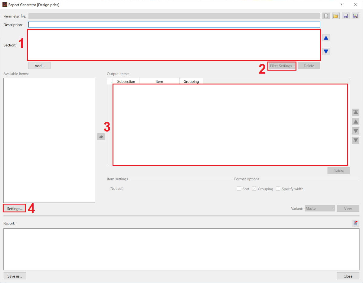
Launch this dialog by clicking Report > User > Report Generator in eCADSTAR PCB Editor, or Report > User > PCB Report Generator in eCADSTAR Schematic Editor. When launching the dialog from eCADSTAR Schematic Editor, a temporary PCB design is created, and is used when generating reports. A progress bar is displayed while it is created. The recommended procedure for creating reports in this dialog is described below. Each step refers to the image below.
- Select a section in the Section box. This value defines the number of rows in the generated report. For example, if you select Board, then only one row is displayed for the board. If you select Component, then a row can be displayed for each component in the design.
- Optionally, filter the displayed attributes using the Filter Settings dialog. The specified filter is applied to each section specified in the Section box.
- In the Output items box, configure the attributes that you add from the Available items box for each section. The number of attributes that you add to the Output items box defines the number of columns that are displayed for each selected section.
- Specify the formatting of the reported data in the Settings dialog. This includes the format of numeric values, the relevant units and the contents of the header and footer. You can also rotate and offset the data, and specify the side of the board.
- When the Report Generator dialog is launched from eCADSTAR Schematic Editor, it searches the current library for a technology file with valid hole layer mapping. A temporary PCB design in then created using this file. However, much of the data generated by the Report Generator command may not be valid in this PCB design.
- If the Use in Layout field is set to NO for a part in the in eCADSTAR Library Editor, Part Editor Panel: Properties tab, then data is not generated for the relevant part when the Report Generator dialog is launched from eCADSTAR Schematic Editor.
- High-Speed attributes cannot be selected in the Report Generator dialog.
| Item | Description | |
|---|---|---|
| Parameter file | The path to the specified parameter file. Parameter files allow you to save the settings that you specify in this dialog to a .prgx file. This allows you to apply the same formatting when generating reports for other designs. | |
 New parameter file New parameter file
|
Allows you to specify a new parameter file. If a parameter
file is currently open, then it is closed. If there are any unsaved
changes in the Report Generator
dialog, then a confirmation dialog is displayed, which prompts
you to save them. Save the new parameter file by clicking  or or
 . . |
|
 Open parameter file Open parameter file
|
Allows you to select an existing parameter file. In the displayed Open dialog, browse to a .prgx file and select Open. The path to the selected file is shown in the Parameter file box. If a parameter file is already selected in the Report Generator dialog and there are unsaved changes, then you are prompted to save the changes. When you first install eCADSTAR, the default location is the installation directory. After you select a parameter file, the default location becomes the last location that it was selected. | |
|
Save parameter file
|
Saves the changes that you specify in the Report Generator dialog. | |
|
Save parameter
file as |
Allows you to save the parameter file using a different name or location. Specify its name and location in the displayed Save As dialog. | |
| Description | This is an optional field which is saved as part of the parameter file. It can be used to describe the type of report that is generated by it. | |
| Section | The Section box displays the elements
that comprise a PCB, which you select in the Add
Section dialog. If you select an item in this box, then the
associated attributes are displayed in the Available
items table. The value that you specify in the Section box defines the number of rows in
the generated report. For example, if you select Board,
then only one row is displayed for the board. If you select Component, then a row can be displayed
for each component in the design. The order that items are listed
in the Section box defines the order
in which the associated attributes are displayed in the Report box. The attributes of items at the
top of the Section box are displayed
first in the Report box. Use the |
|
| Board | If you select Board in the Add Section dialog, then only attributes related to the board can be selected in the Available items table. Board is displayed in the Section box. | |
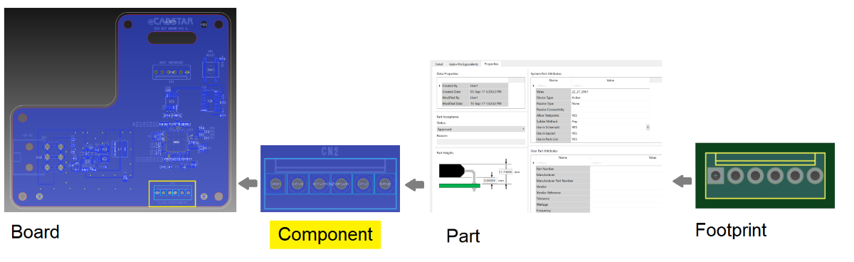
| Component | As a component is part of the board, and comprises a part and
a footprint, attributes of the board, part and footprint can be
selected in the Available
items table, as well as those of the component and
component groups. These are displayed in the relevant sub-sections
in the in the Available
items table. Component is
displayed in the Section box.
|
|
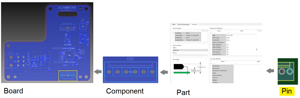
| Pin |
As a pin is part of a component, which is an instance of a part, and a component is part of the board, attributes of the component, part and board can be selected in the Available items table, as well as those of the pin and associated net. These are displayed in the relevant sub-sections in the in the Available items table. Pin is displayed in the Section box.
|
|
| Padstack | If you select Padstack in the Add Section dialog, then attributes related to padstacks and their associated nets can be selected in the Available items table. These are displayed in the relevant sub-sections in the in the Available items table. Padstack is displayed in the Section box. As padstacks are associated only with the board, they are available as a self-contained item in the Available items table. | |
| Hole | If you select Hole in the Add Section dialog, then only attributes related to holes on the board can be selected in the Available items table. Hole is displayed in the Section box. As holes are associated only with the board, they are available as a self-contained item in the Available items table. | |
|
|
The item that you select in the Section box is moved up a place in this box. The order that items are listed in the Section box defines the order in which the associated attributes are displayed in the Report box. The attributes of items at the top of the Section box are displayed first in the Report box. | |
|
|
The item that you select in the Section box is moved down a place in this box. The order that items are listed in the Section box defines the order in which the associated attributes are displayed in the Report box. The attributes of items at the top of the Section box are displayed first in the Report box. | |
| Add | Displays the Add Section dialog. Alternatively, right-click in the Section box and select Add Section on the assist menu. This dialog allows you to add the following elements that comprise a PCB to the Section box. If you select an item in the Section box, then the associated attributes are displayed in the Available items table. | |
| Filter Settings | Displays the Filter Settings dialog. Alternatively, right-click in the Section box and select Filter Settings on the assist menu. For an item that you select in the Section box, this dialog allows you to optionally filter the attribute values that are displayed in the Report box. The settings that you specify are saved if you save the parameter file. | |
| Delete | Deletes the item that you select in the Section box. Alternatively, right-click in the Section box and select Delete Section on the assist menu. If you have selected attributes that are associated with the section, then a confirmation dialog is displayed. |
Available items
| Item | Description |
|---|---|
| Available items table | The attributes that are associated with the element of the
PCB that you specify in the Section
box. These are displayed in relevant sub-sections, which are formatted
as follows: "-----[Subsection] -----". The Format
elements item is also displayed, which allows you to specify
a string, display attributes on separate rows and add blank rows
between them. The attributes in the sub-sections shown below can
be reported on by moving them to the Output
items table. The attributes are displayed, in the specified
order, in the Report box when you
click View or  . . |

|
Moves the item that you select in the Available items table to the Output items table. You can select multiple items using the Ctrl or Shift key, or by dragging the cursor in the Available items table. |
| Settings | Displays the Report Generator: Settings dialog. This dialog allows you to specify the formatting of the data that you generate in the Report Generator dialog, including the information in the header and footer. |
Board
If Board is selected in the Add Section dialog, then the following fields are displayed in the Available items section. These allow you to report on information for the board by adding the required fields to the Output items table. By default, this information is displayed as a single row in the Report box.
| Item | Value | Description | |
|---|---|---|---|
| Board | Absolute Path | String | Displays the location of the design file as a complete path from the root location. |
| Technology Name | String | In eCADSTAR PCB Editor, the name of the technology is shown that is associated with the design. This value is shown in the Technology Editor Dialog, Technology name field. When running the Report Generator command in eCADSTAR Schematic Editor, the technology file is not necessarily associated with the current design. Consequently, this attribute may not be valid in the generated PCB design. | |
| Board Size | Comma-separated real numbers | In eCADSTAR PCB Editor, the X and Y dimensions are shown for the board. For example, "90.000, 80,000". In eCADSTAR Schematic Editor, this attribute may not be valid in the generated PCB design. | |
| Board Size: Width | Real number | In eCADSTAR PCB Editor, the X dimension of the board is shown. In eCADSTAR Schematic Editor, In eCADSTAR Schematic Editor, this attribute may not be valid in the generated PCB design. | |
| Board Size: Height | Real number | In eCADSTAR PCB Editor, the Y dimension of the board is shown. In eCADSTAR Schematic Editor, In eCADSTAR Schematic Editor, this attribute may not be valid in the generated PCB design. | |
| Coordinates (Bottom-Left) | Coordinates | In eCADSTAR PCB Editor, the coordinates are shown for the bottom-left corner of the board outline. In eCADSTAR Schematic Editor, In eCADSTAR Schematic Editor, this attribute may not be valid in the generated PCB design. | |
| Coordinate (Left) X | Real number | In eCADSTAR PCB Editor, the X coordinate is shown for the bottom-left corner of the board outline. In eCADSTAR Schematic Editor, this attribute may not be valid in the generated PCB design. | |
| Coordinate (Bottom) Y | Real number | In eCADSTAR PCB Editor, the Y coordinate is shown for the bottom-left corner of the board outline. In eCADSTAR Schematic Editor, this attribute may not be valid in the generated PCB design. | |
| Coordinates (Top-right) | Coordinates | In eCADSTAR PCB Editor, the coordinates are shown for the top-right corner of the board outline. In eCADSTAR Schematic Editor, this attribute may not be valid in the generated PCB design. | |
| Coordinate (Right) X | Real number | In eCADSTAR PCB Editor, the X coordinate is shown for the top-right corner of the board outline. In eCADSTAR Schematic Editor, this attribute may not be valid in the generated PCB design. | |
| Coordinate (Top) Y | Real number | In eCADSTAR PCB Editor, the Y coordinate is shown for the top-right corner of the board outline. In eCADSTAR Schematic Editor, this attribute may not be valid in the generated PCB design. | |
| Component Group Count | Integer | In eCADSTAR PCB Editor, the number of Component Groups in the design is displayed. In eCADSTAR Schematic Editor, this attribute may not be valid in the generated PCB design. | |
| Component Count | Integer | The total number of components for all variations of the design.
Note If you select the Component Count attribute in the Component section, then the total number of components is shown only for the currently-selected variant. |
|
| Net Count | Integer | The number of nets in the design. | |
| Conductor Layer Count | Integer | In eCADSTAR PCB Editor, the number of conductor layers in the design is displayed. Conductor layers are added to the design using the Technology Library Editor dialog. In eCADSTAR Schematic Editor, this attribute may not be valid in the generated PCB design. | |
| Hole Count | Integer | In eCADSTAR PCB Editor, the number of holes in the board is displayed. In eCADSTAR Schematic Editor, this attribute may not be valid in the generated PCB design. | |
| Format elements | Text | String | Allows you to specify any text or symbol in the Strings box that is displayed in the Item Settings section. The specified content is shown for each row in the Report box, in the position specified in the Output items table. |
| Line Break | Not applicable | For the attributes in the Output items table, selecting
Line break item allows you to
display them on separate rows, and add blank rows between them.
|
Component
If Component is selected in the Add Section dialog, then the following fields are displayed in the Available items section. These allow you to report on information for all components in the design by adding the required fields to the Output items table.
| Item | Value | Description | |
|---|---|---|---|
| Component | Reference Designator | String | The reference designators for all components in the design. See Changing a Reference Designator. |
| Placement Status | PLACED or UNPLACED. | In eCADSTAR PCB Editor,
the placement status of the components on the board are displayed
as either PLACED or UNPLACED.
In eCADSTAR Schematic Editor, this attribute may not be valid in the generated PCB design. |
|
| Placement Side | A-SIDE or B-SIDE | In eCADSTAR PCB Editor,
the side of the board is displayed on which each component is
placed.
In eCADSTAR Schematic Editor, this attribute may not be valid in the generated PCB design. |
|
| Fixed | YES or NO | In eCADSTAR PCB Editor,
objects on the canvas can be fixed so that they cannot be edited.
This is done using the Fix
command. A fixed object cannot be modified, moved or deleted.
See Fixing a Selected
Object.
In eCADSTAR Schematic Editor, this attribute may not be valid in the generated PCB design. |
|
| Jumper | ON or OFF | Indicates whether a component is a jumper. This is specified
for the part in the Part
Editor Panel: Detail tab, in eCADSTAR Library Editor.
|
|
| Decoupling Capacitor | TRUE or FALSE | Indicates whether a component is a decoupling capacitor (decap).
These are created in eCADSTAR PCB Editor
using the Decoupling
Capacitor command.
|
|
| Decoupling Capacitor Count | Integer | In eCADSTAR PCB Editor, the number of decoupling capacitors (decaps) is shown for each component in the design. In eCADSTAR Schematic Editor, this attribute may not be valid in the generated PCB design. | |
| Group Net Display | ON or OFF | In eCADSTAR PCB Editor,
this attribute indicates whether the Group
net display attribute is set for a component. This is set
in the Properties
Panel in eCADSTAR PCB Editor.
In eCADSTAR Schematic Editor, this attribute may not be valid in the generated PCB design. |
|
| Placed | TRUE or FALSE | In eCADSTAR PCB Editor,
this field indicates whether a component is placed inside or outside
of the board outline.
In eCADSTAR Schematic Editor, this attribute may not be valid in the generated PCB design. |
|
| Placement Coordinates | Coordinates | In eCADSTAR PCB Editor, the X and Y values of the placement coordinates are shown for each component in the design. In eCADSTAR Schematic Editor, this attribute may not be valid in the generated PCB design. The Report Generator: Settings dialog, Format tab, allows you to specify the formatting of the displayed coordinates. | |
| Placement Coordinate X | Coordinates | In eCADSTAR PCB Editor, the X value of the placement coordinates is shown for each component in the design. In eCADSTAR Schematic Editor, this attribute may not be valid in the generated PCB design. The Report Generator: Settings dialog, Format tab, allows you to specify the formatting of the displayed coordinates. | |
| Placement Coordinate Y | Coordinates | In eCADSTAR PCB Editor, the Y value of the placement coordinates is shown for each component in the design. In eCADSTAR Schematic Editor, this attribute may not be valid in the generated PCB design. The Report Generator: Settings dialog, Format tab, allows you to specify the formatting of the displayed coordinates. | |
| Placement Angle | Integer | In eCADSTAR PCB Editor, the placement angle is shown for each component. In eCADSTAR Schematic Editor, this attribute may not be valid in the generated PCB design. | |
| Pin Count | Integer | The number of pins is shown for each component. | |
| Component Symbol | String | Allows you to show the component symbols on the layer that
you specify in the Item settings
section. The Layer name box in the
Item settings section is made available.
The following layers, on which component symbols can be added,
can be selected.
|
|
| Component Symbol Coordinates | Coordinates | In eCADSTAR PCB Editor,
the Component symbol coordinates attribute
allows you to show the X and Y coordinates for component symbols
on the layer specified in the Item settings
section. The Layer name box in the
Item settings section is made available.
The following layers, on which component symbols can be added,
can be selected.
In eCADSTAR Schematic Editor, this attribute may not be valid in the generated PCB design. The Report Generator: Settings dialog, Format tab, allows you to specify the formatting of the displayed coordinates. |
|
| Component Symbol Coordinate X | Coordinates | In eCADSTAR PCB Editor,
the Component symbol coordinates X
attribute allows you to show the X value of the coordinates
for component symbols. This value is shown for the layer specified
in the Item settings section. The
Layer name box in the Item
settings section is made available. The following layers,
on which component symbols can be added, can be selected.
In eCADSTAR Schematic Editor, this attribute may not be valid in the generated PCB design. The Report Generator: Settings dialog, Format tab, allows you to specify the formatting of the displayed coordinates. |
|
| Component Symbol Coordinate Y | Coordinates | In eCADSTAR PCB Editor,
the Component symbol coordinates Y
attribute allows you to show the Y value of the coordinates
for component symbols. This value is shown for the layer specified
in the Item settings section. The
Layer name box in the Item
settings section is made available. The following layers,
on which component symbols can be added, can be selected.
In eCADSTAR Schematic Editor, this attribute may not be valid in the generated PCB design. The Report Generator: Settings dialog, Format tab, allows you to specify the formatting of the displayed coordinates. |
|
| Component Strings | Allows you to show any text that you add to a footprint in Footprint Editor, for the layer specified in the Item settings section. The Layer name box in the Item settings section is made available. Any symbol layer or user-defined layer can be selected. If you select the layer on which the text is added, for the relevant side of the board, then the added text is shown in the Report box. | ||
| Component Strings Coordinates | Coordinates | In eCADSTAR PCB Editor, the X and Y coordinates are shown for any text that you add to a footprint in Footprint Editor, for the layer specified in the Item settings section. The Layer name box in the Item settings section is made available. Any symbol layer or user-defined layer can be selected. If you select the layer on which the text is added, for the relevant side of the board, then the coordinates are shown in the Report box. In eCADSTAR Schematic Editor, this attribute may not be valid in the generated PCB design. The Report Generator: Settings dialog, Format tab, allows you to specify the formatting of the displayed coordinates. | |
| Component Strings Coordinate X | Coordinates | In eCADSTAR PCB Editor, the X value of the coordinates is shown for any text that you add to a footprint in Footprint Editor, for the layer specified in the Item settings section. The Layer name box in the Item settings section is made available. Any symbol layer or user-defined layer can be selected. If you select the layer on which the text is added, for the relevant side of the board, then the coordinate value is shown in the Report box. In eCADSTAR Schematic Editor, this attribute may not be valid in the generated PCB design. The Report Generator: Settings dialog, Format tab, allows you to specify the formatting of the displayed coordinates. | |
| Component Strings Coordinate Y | Coordinates | In eCADSTAR PCB Editor, the Y value of the coordinates is shown for any text that you add to a footprint in Footprint Editor, for the layer specified in the Item settings section. The Layer name box in the Item settings section is made available. Any symbol layer or user-defined layer can be selected. If you select the layer on which the text is added, for the relevant side of the board, then the coordinate value is shown in the Report box. In eCADSTAR Schematic Editor, this attribute may not be valid in the generated PCB design. The Report Generator: Settings dialog, Format tab, allows you to specify the formatting of the displayed coordinates. | |
| Component Placement Height (Standoff) | Real number | The stand-off value is shown for the component on either Side A or Side B of the board. This value is specified in the Part Heights section of the Part Editor Panel: Properties tab, in eCADSTAR Library Editor. | |
| Component Placement Height A (Standoff) | Real number | For a component that is placed on Side A of the board, its stand-off value is shown. This value is specified in the Part Heights section of the Part Editor Panel: Properties tab, in eCADSTAR Library Editor. You can specify the placement side for a component in the Placement Side box in the Properties Panel. | |
| Component Placement Height B (Standoff) | Real number | For a component that is placed on Side B of the board, its stand-off value is shown. This value is specified in the Part Heights section of the Part Editor Panel: Properties tab, in eCADSTAR Library Editor. You can specify the placement side for a component in the Placement Side box in the Properties Panel. | |
| Component Placement Height (Maximum) | Real number | The maximum allowable height is shown for the component on either Side A or Side B of the board. This value is specified in the Part Heights section of the Part Editor Panel: Properties tab, in eCADSTAR Library Editor. | |
| Component Placement Height A (Maximum) | Real number | For a component that is placed on Side A of the board, its maximum allowable height is shown. This value is specified in the Part Heights section of the Part Editor Panel: Properties tab, in eCADSTAR Library Editor. You can specify the placement side for a component in the Placement Side box in the Properties Panel. | |
| Component Placement Height B (Maximum) | Real number | For a component that is placed on Side B of the board, its maximum allowable height is shown. This value is specified in the Part Heights section of the Part Editor Panel: Properties tab, in eCADSTAR Library Editor. You can specify the placement side for a component in the Placement Side box in the Properties Panel. | |
| Count | Integer | If you specify that the items in the Report
box are grouped, then the total number is shown for the
attribute on which the report is grouped by. If the items in the
Report box are not grouped, then a
value of "1" is shown for each row in the Report
box.
Note
|
|
| User Attribute | Shows the system attributes and user-defined attributes for the component. These are set in the Part Editor Panel: Properties tab or in the Library Editor Panel: Parts tab, in the library. If you specify attributes in Constraint Browser, then these are also displayed. The User attribute name box is displayed in the Item settings section. This allows you to select the system attribute or user-defined attribute that you want to display. User-defined attributes are defined in the Attribute Manager dialog. | ||
| Part | Part Name | String | The part name that is associated with each component in the design. |
| Part Acceptance Status | APPROVED or UNAPPROVED | Indicates the approval status of each part in the design. This
is specified in the Part Acceptance
section of the Part
Editor Panel: Properties tab, in eCADSTAR Library Editor.
|
|
| Part Acceptance Reason | String | Indicates the reason that is entered for non-approval of the part in the design. This is specified in the Part Acceptance section, Reason box, in the Part Editor Panel: Properties tab, in eCADSTAR Library Editor. | |
| Star Point | TRUE or FALSE | Indicates whether a component is a star point. Star points
can be used to connect multiple signals. These are created in
the Part Information section
of the Part
Editor Panel: Detail tab, in eCADSTAR Library Editor.
See Creating
a Star Point.
|
|
| Jumper | ON or OFF | Indicates whether a part is a jumper. This is specified in
the Part
Editor Panel: Detail tab, in eCADSTAR Library Editor.
|
|
| Solder Method | Reflow, Single Reflow or Any | Displays whether the solder method for the part is restricted to "Reflow" or "Single Reflow", or whether it is set to "Any", to allow any method of soldering. This value is specified in the Solder Method field in the Library Editor Panel: Parts tab, or the Part Editor Panel: Properties tab. | |
| Use in Schematic | TRUE or FALSE | In eCADSTAR PCB Editor,
this attribute displays whether the part can be back-annotated
into eCADSTAR Schematic Editor.
This value is specified in the Use
in Schematic field, in the Library
Editor Panel: Parts tab, or the Part
Editor Panel: Properties tab.
In eCADSTAR Schematic Editor, this attribute may not be valid in the generated PCB design. |
|
| Use in Layout | TRUE or FALSE | In eCADSTAR PCB Editor,
this attribute displays whether the part can be forward annotated
into eCADSTAR PCB Editor.
This value is specified in the Use
in Layout field, in the Library
Editor Panel: Parts tab, or the Part
Editor Panel: Properties tab.
In eCADSTAR Schematic Editor, this attribute may not be valid in the generated PCB design. |
|
| Use in Parts List | TRUE or FALSE | Displays whether the part appears in the part lists that you
generate in eCADSTAR. This value is specified in the Use
in Parts List, in the Library
Editor Panel: Parts tab, or the Part
Editor Panel: Properties tab.
|
|
| Pin Swapping | ON or OFF | Displays whether pin swapping is allowed for a part. If pin
swapping is allowed, then groups of pins are defined for it which
have the same function and can therefore be swapped to improve
the layout process. For example, two input pins of an "AND"
gate. This is defined in the Part
Editor Panel: Gate+Pin Equivalents tab.
|
|
| Created By | String | Displays the name of the user who created the part. This value is displayed in the Part Editor Panel: Properties tab. | |
| Created Date | String | Displays the date and time that the part was created. This value is displayed in the Part Editor Panel: Properties tab. | |
| Modified By | String | Displays the name of the user who last modified the part. This value is displayed in the Part Editor Panel: Properties tab. | |
| Modified Date | String | Displays the date and time that the part was last modified. This value is displayed in the Part Editor Panel: Properties tab. | |
| User Attribute | String | Shows the system attributes and user-defined attributes for the part. These are set in the Part Editor Panel: Properties tab or in the Library Editor Panel: Parts tab, in the library. If you specify attributes in Constraint Browser, then these are also displayed. The User attribute name box is displayed in the Item settings section. This allows you to select the system attribute or user-defined attribute that you want to display. User-defined attributes are defined in the Attribute Manager dialog. | |
| Footprint | Footprint Name | String | Displays the footprint that is associated with each part. This value is specified in the Footprint Attributes Panel in Footprint Editor. |
| Created By | String | Displays the name of the user who created the footprint. This value is specified in the Footprint Attributes Panel in Footprint Editor. | |
| Created Date | String | Displays the date and time that the footprint was created. This value is specified in the Footprint Attributes Panel in Footprint Editor. | |
| Modified By | String | Displays the name of the user who last modified the footprint. This value is specified in the Footprint Attributes Panel in Footprint Editor. | |
| Modified Date | String | Displays the date and time that the footprint was last modified. This value is specified in the Footprint Attributes Panel in Footprint Editor. | |
| User Attribute | Allows you to show the 3D model that is set in the Footprint Attributes Panel for the footprint. The User attribute name box is displayed in the Item settings section. This allows you to select the attribute that you want to display. | ||
| Component group | Component Group Name | In eCADSTAR PCB Editor,
if a component is a member of a component group, then the name
of the component group is displayed. Component groups are specified
in the Component
Group Settings dialog.
In eCADSTAR Schematic Editor, this attribute may not be valid in the generated PCB design. |
|
| Component Group Coordinates | In eCADSTAR PCB Editor, the X and Y values of the coordinates are shown for each component group. Component groups are specified in the Component Group Settings dialog. In eCADSTAR Schematic Editor, this attribute may not be valid in the generated PCB design. The Report Generator: Settings dialog, Format tab, allows you to specify the formatting of the displayed coordinates. | ||
| Component Group Coordinate X | In eCADSTAR PCB Editor, the X value of the coordinates is shown for each component group. Component groups are specified in the Component Group Settings dialog. In eCADSTAR Schematic Editor, this attribute may not be valid in the generated PCB design. The Report Generator: Settings dialog, Format tab, allows you to specify the formatting of the displayed coordinates. | ||
| Component Group Coordinate Y | In eCADSTAR PCB Editor, the Y value of the coordinates is shown for each component group. Component groups are specified in the Component Group Settings dialog. In eCADSTAR Schematic Editor, this attribute may not be valid in the generated PCB design. The Report Generator: Settings dialog, Format tab, allows you to specify the formatting of the displayed coordinates. | ||
| Board | Absolute Path | String | In eCADSTAR PCB Editor, the location of the design file is displayed as a complete path from the root location. In eCADSTAR Schematic Editor, the path is not valid in the generated PCB design. |
| Technology Name | String | In eCADSTAR PCB Editor, the name of the technology is shown that is associated with the design. This value is shown in the Technology Editor Dialog, Technology name field. In eCADSTAR Schematic Editor, this attribute may not be valid in the generated PCB design. | |
| Placement Coordinates | Coordinates | In eCADSTAR PCB Editor, the X and Y values of the placement coordinates are shown for each component in the design. In eCADSTAR Schematic Editor, this attribute may not be valid in the generated PCB design. The Report Generator: Settings dialog, Format tab, allows you to specify the formatting of the displayed coordinates. | |
| Placement Coordinate X | Coordinates | In eCADSTAR PCB Editor, the X value of the placement coordinates is shown for the board. In eCADSTAR Schematic Editor, this attribute may not be valid in the generated PCB design. The Report Generator: Settings dialog, Format tab, allows you to specify the formatting of the displayed coordinates. | |
| Placement Coordinate Y | Coordinates | In eCADSTAR PCB Editor, the Y value of the placement coordinates is shown for the board. In eCADSTAR Schematic Editor, this attribute may not be valid in the generated PCB design. The Report Generator: Settings dialog, Format tab, allows you to specify the formatting of the displayed coordinates. | |
| Board Size | Comma-separated real numbers | In eCADSTAR PCB Editor, the X and Y dimensions are shown for the board. For example, "90.000, 80,000". In eCADSTAR Schematic Editor, this attribute may not be valid in the generated PCB design. | |
| Board Size: Width | Real number | In eCADSTAR PCB Editor, the X dimension of the board is shown. In eCADSTAR Schematic Editor, this attribute may not be valid in the generated PCB design. | |
| Board Size: Height | Real number | In eCADSTAR PCB Editor, the Y dimension of the board is shown. In eCADSTAR Schematic Editor, this attribute may not be valid in the generated PCB design. | |
| Coordinates (Bottom-Left) | Coordinates | In eCADSTAR PCB Editor, the coordinates are shown for the bottom-left corner of the board outline. In eCADSTAR Schematic Editor, this attribute may not be valid in the generated PCB design. | |
| Coordinate (Left) X | Real number | In eCADSTAR PCB Editor, the X coordinate is shown for the bottom-left corner of the board outline. In eCADSTAR Schematic Editor, this attribute may not be valid in the generated PCB design. | |
| Coordinate (Bottom) Y | Real number | In eCADSTAR PCB Editor, the Y coordinate is shown for the bottom-left corner of the board outline. In eCADSTAR Schematic Editor, this attribute may not be valid in the generated PCB design. | |
| Coordinates (Top-right) | Coordinates | In eCADSTAR PCB Editor, the coordinates are shown for the top-right corner of the board outline. In eCADSTAR Schematic Editor, this attribute may not be valid in the generated PCB design. | |
| Coordinate (Right) X | Real number | In eCADSTAR PCB Editor, the X coordinate is shown for the top-right corner of the board outline. In eCADSTAR Schematic Editor, this attribute may not be valid in the generated PCB design. | |
| Coordinate (Top) Y | Real number | In eCADSTAR PCB Editor, the Y coordinate is shown for the top-right corner of the board outline. In eCADSTAR Schematic Editor, this attribute may not be valid in the generated PCB design. | |
| Component Group Count | Integer | In eCADSTAR PCB Editor, the number of component groups in the design is displayed. | |
| Component Count | Integer | The total number of components for the currently-selected variant.
Note If you select the Component Count attribute in the Board section, then the total number of components is shown for all variants in the design. |
|
| Net Count | Integer | The number of nets in the design. | |
| Conductor Layer Count | Integer | In eCADSTAR PCB Editor, the number of conductor layers in the design is displayed. Conductor layers are added to the design using the Technology Library Editor dialog. In eCADSTAR Schematic Editor, this attribute may not be valid in the generated PCB design. | |
| Hole Count | Integer | In eCADSTAR PCB Editor, the number of holes in the board is displayed. In eCADSTAR Schematic Editor, this attribute may not be valid in the generated PCB design. | |
| Format elements | Text | String | Allows you to specify any text or symbol in the Strings box that is displayed in the Item Settings section. The specified content is shown for each row in the Report box, in the position specified in the Output items table. |
| Line Break | Not applicable | For the attributes in the Output items table, selecting
Line break item allows you to
display them on separate rows, and add blank rows between them.
|
Pin
If Pin is selected in the Add Section dialog, then the following fields are displayed in the Available items section. These allow you to report on information for all pins in the design by adding the required fields to the Output items table.
| Item | Value | Description | |
|---|---|---|---|
| Pin | Pin Name | String | The name of each pin in the design. This value is displayed in the Properties Panel, Pin Name field when you select a padstack on the canvas in eCADSTAR PCB Editor. |
| Pin Number | String | The number of each pin in the design. This value is displayed in the Properties Panel, Pin Number field when you select a padstack on the canvas in eCADSTAR PCB Editor. | |
| Pin Coordinates | Coordinates | In eCADSTAR PCB Editor, the coordinates are displayed of each pin in the design. This value is displayed in the Properties Panel, Coordinates field when you select a padstack on the canvas in eCADSTAR PCB Editor. In eCADSTAR Schematic Editor, this attribute may not be valid in the generated PCB design. | |
| Pin Coordinate X | Coordinates | In eCADSTAR PCB Editor, the X value of the coordinates is displayed for each pin in the design. The coordinates of a pin are displayed in the Properties Panel, Coordinates field when you select a padstack on the canvas in eCADSTAR PCB Editor. In eCADSTAR Schematic Editor, this attribute may not be valid in the generated PCB design. | |
| Pin Coordinate Y | Coordinates | In eCADSTAR PCB Editor, the Y value is displayed of the coordinates for each pin in the design. The coordinates of a pin are displayed in the Properties Panel, Coordinates field when you select a padstack on the canvas in eCADSTAR PCB Editor. In eCADSTAR Schematic Editor, this attribute may not be valid in the generated PCB design. | |
| Pin Type | UNDEFINPUTOUTPUTBIDIRECTPOWERGROUNDUNCONNECTED | The type of each pin in the design. This value is displayed
in the Properties
Panel, Pin Type field when you select a padstack on the
canvas in eCADSTAR PCB Editor.
Pin types are specified in the Part
Editor Panel: Detail tab.
|
|
| Figure | PADSTACK | Displays the object on which the pin is placed in the design.
The following types of object may be listed in the Report
box.
|
|
| Figure Name | String | Displays the name of the object on which the pin is placed
in the design. Names for the following types of object may be
listed in the Report box.
|
|
| Through Hole | TRUE or FALSE | In eCADSTAR PCB Editor,
this attribute indicates whether the padstack that is associated
with a pin is a through hole or surface mount padstack.
In eCADSTAR Schematic Editor, this attribute may not be valid in the generated PCB design. |
|
| Count | Integer |
If you specify that the items in the Report box are grouped, then the total number is shown for the attribute on which the report is grouped by. If the items in the Report box are not grouped, then a value of "1" is shown for each row in the Report box. Note
Specify that items in the Report box are grouped by selecting Grouping in the Format options section, and then selecting the Grouping check box in the Output items table for the items that you want to group by. |
|
| User Attribute | The user attributes that you set for the relevant pin in the Part Editor Panel: Properties tab or in the Library Editor Panel: Parts tab, in the library. If you specify attributes in Constraint Browser, then these are also displayed. User-defined attributes are defined in the Attribute Manager dialog. | ||
| Net | Name | String | If a net is associated with a pin, then it is displayed for each pin in the design. |
| Type | GROUNDSIGNALPOWERTEMPORARY | The type of net that is associated with each pin.
|
|
| Component | Reference Designator | String | The reference designators for all components in the design. See Changing a Reference Designator. |
| Placement Status | PLACED or UNPLACED. | In eCADSTAR PCB Editor, the placement status of the components on the board is displayed as either PLACED or UNPLACED. In eCADSTAR Schematic Editor, this attribute may not be valid in the generated PCB design. | |
| Placement Side | A-SIDE or B-SIDE | In eCADSTAR PCB Editor,
the side of the board is displayed on which each component is
placed.
In eCADSTAR Schematic Editor, this attribute may not be valid in the generated PCB design. |
|
| Fixed | YES or NO | In eCADSTAR PCB Editor,
objects on the canvas can be fixed so that they cannot be edited.
This is done using the Fix
command. A fixed object cannot be modified, moved or deleted.
See Fixing a Selected
Object.
In eCADSTAR Schematic Editor, this attribute may not be valid in the generated PCB design. |
|
| Jumper | ON or OFF | Indicates whether a component is a jumper. This is specified
in the Part
Editor Panel: Detail tab, in eCADSTAR Library Editor.
|
|
| Decoupling Capacitor | TRUE or FALSE | Indicates whether a component is a decoupling capacitor (decap).
These are created in eCADSTAR PCB Editor
using the Decoupling
Capacitor command.
In eCADSTAR Schematic Editor, this attribute may not be valid in the generated PCB design. |
|
| Decoupling Capacitor count | Integer | In eCADSTAR PCB Editor, the number of decoupling capacitors (decaps) is displayed for each component in the design. In eCADSTAR Schematic Editor, this attribute may not be valid in the generated PCB design. | |
| Group net display | ON or OFF | In eCADSTAR PCB Editor,
this attribute displays whether the Group
net display attribute is set for a component. This is set
in the Properties
Panel in eCADSTAR PCB Editor.
In eCADSTAR Schematic Editor, this attribute may not be valid in the generated PCB design. |
|
| Placed | TRUE or FALSE | In eCADSTAR PCB Editor,
this attribute indicates whether a component is placed inside
or outside of the board outline.
In eCADSTAR Schematic Editor, this attribute may not be valid in the generated PCB design. |
|
| Placement coordinates | Coordinates | In eCADSTAR PCB Editor, the X and Y values of the placement coordinates are shown for each component in the design.In eCADSTAR Schematic Editor, this attribute may not be valid in the generated PCB design. The Report Generator: Settings dialog, Format tab, allows you to specify the formatting of the displayed coordinates. | |
| Placement coordinate X | Coordinates | In eCADSTAR PCB Editor, the X value of the placement coordinates is shown for each component in the design. In eCADSTAR Schematic Editor, this attribute may not be valid in the generated PCB design. The Report Generator: Settings dialog, Format tab, allows you to specify the formatting of the displayed coordinates. | |
| Placement coordinate Y | Coordinates | In eCADSTAR PCB Editor, the Y value of the placement coordinates is shown for each component in the design.In eCADSTAR Schematic Editor, this attribute may not be valid in the generated PCB design. The Report Generator: Settings dialog, Format tab, allows you to specify the formatting of the displayed coordinates. | |
| Placement angle | Integer | In eCADSTAR PCB Editor, the placement angle of each component is shown. In eCADSTAR Schematic Editor, this attribute may not be valid in the generated PCB design. | |
| Pin count | Integer | The number of pins is shown for each component. | |
| Component symbol | String | Allows you to show the component symbols on the layer that
you specify in the Item settings
section. The Layer name box in the
Item settings section is made
available. The following layers, on which component symbols can
be added, can be selected.
|
|
| Component symbol coordinates | Coordinates | In eCADSTAR PCB Editor,
the Component symbol coordinates attribute
allows you to show the X and Y coordinate values for component
symbols on the layer specified in the Item
settings section. The Layer name
box in the Item settings section
is made available. The following layers, on which component symbols
can be added, can be selected.
In eCADSTAR Schematic Editor, this attribute may not be valid in the generated PCB design. values. The Report Generator: Settings dialog, Format tab, allows you to specify the formatting of the displayed coordinates. |
|
| Component symbol coordinate X | Coordinates | In eCADSTAR PCB Editor,
the Component symbol coordinates X
attribute allows you to show the X value of the coordinates
for component symbols. This value is shown for the layer specified
in the Item settings section.
The Layer name box in the Item
settings section is made available. The following layers,
on which component symbols can be added, can be selected.
In eCADSTAR Schematic Editor, this attribute may not be valid in the generated PCB design. values. The Report Generator: Settings dialog, Format tab, allows you to specify the formatting of the displayed coordinates. |
|
| Component symbol coordinate Y | Coordinates | In eCADSTAR PCB Editor,
the Component symbol coordinates Y
attribute allows you to show the Y value of the coordinates
for component symbols. This value is shown for the layer specified
in the Item settings section. The
Layer name box in the Item
settings section is made available. The following layers,
on which component symbols can be added, can be selected.
In eCADSTAR Schematic Editor, this attribute may not be valid in the generated PCB design. values. The Report Generator: Settings dialog, Format tab, allows you to specify the formatting of the displayed coordinates. |
|
| Component strings | Allows you to show any text that you add to a footprint in Footprint Editor, for the layer specified in the Item settings section. The Layer name box in the Item settings section is made available. Any symbol layer or user-defined layer can be selected. If you select the layer on which the text is added, for the relevant side of the board, then the added text is shown in the Report box. | ||
| Component strings coordinates | Coordinates | In eCADSTAR PCB Editor, the X and Y values of the coordinates are shown for any text that you add to a footprint in Footprint Editor, for the layer specified in the Item settings section. The Layer name box in the Item settings section is made available. Any symbol layer or user-defined layer can be selected. If you select the layer on which the text is added, for the relevant side of the board, then the coordinates are shown in the Report box. In eCADSTAR Schematic Editor, this attribute may not be valid in the generated PCB design. The Report Generator: Settings dialog, Format tab, allows you to specify the formatting of the displayed coordinates. | |
| Component strings coordinate X | Coordinates | In eCADSTAR PCB Editor, the X value of the coordinates is shown for any text that you add to a footprint in Footprint Editor, for the layer specified in the Item settings section. The Layer name box in the Item settings section is made available. Any symbol layer or user-defined layer can be selected. If you select the layer on which the text is added, for the relevant side of the board, then the coordinate value is shown in the Report box. In eCADSTAR Schematic Editor, this attribute may not be valid in the generated PCB design. The Report Generator: Settings dialog, Format tab, allows you to specify the formatting of the displayed coordinates. | |
| Component strings coordinate Y | Coordinates | In eCADSTAR PCB Editor, the Y value of the coordinates is shown for any text that you add to a footprint in Footprint Editor, for the layer specified in the Item settings section. The Layer name box in the Item settings section is made available. Any symbol layer or user-defined layer can be selected. If you select the layer on which the text is added, for the relevant side of the board, then the coordinate value is shown in the Report box. In eCADSTAR Schematic Editor, this attribute may not be valid in the generated PCB design. The Report Generator: Settings dialog, Format tab, allows you to specify the formatting of the displayed coordinates. | |
| Component placement height (Standoff) | Real number | The stand off value is shown for the component. This is specified in the Part Heights section of the Part Editor Panel: Properties tab, in eCADSTAR Library Editor. | |
| Component placement height A (Standoff) | Real number | For a component that is placed on Side A of the board, its stand-off value is shown. This value is specified in the Part Heights section of the Part Editor Panel: Properties tab, in eCADSTAR Library Editor. You can specify the placement side for a component in the Placement Side box in the Properties Panel. | |
| Component placement height B (Standoff) | Real number | For a component that is placed on Side B of the board, its stand-off value is shown. This value is specified in the Part Heights section of the Part Editor Panel: Properties tab, in eCADSTAR Library Editor. You can specify the placement side for a component in the Placement Side box in the Properties Panel. | |
| Component placement height (maximum) | Real number | The maximum height is shown for the component. This is specified in the Part Heights section of the Part Editor Panel: Properties tab, in eCADSTAR Library Editor. | |
| Component placement height A (maximum) | Real number | The maximum height is shown for the component for side A of the board. This is specified in the Part Heights section of the Part Editor Panel: Properties tab, in eCADSTAR Library Editor. | |
| Component placement height B (maximum) | Real number | For a component that is placed on Side B of the board, its maximum allowable height is shown. This value is specified in the Part Heights section of the Part Editor Panel: Properties tab, in eCADSTAR Library Editor. You can specify the placement side for a component in the Placement Side box in the Properties Panel. | |
| User attribute | Shows the system attributes and user-defined attributes for the component. These are set in the Part Editor Panel: Properties tab or in the Library Editor Panel: Parts tab, in the library. If you specify attributes in Constraint Browser, then these are also displayed. The User attribute name box is displayed in the Item settings section. This allows you to select the system attribute or user-defined attribute that you want to display. User-defined attributes are defined in the Attribute Manager dialog. | ||
| Part | Part name | String | The part name that is associated with each component in the design. |
| Part acceptance status | APPROVED or UNAPPROVED | The approval status of each part in the design. This is specified
in the Part Acceptance section
of the Part
Editor Panel: Properties tab, in eCADSTAR Library Editor.
|
|
| Star Point | TRUE or FALSE | Indicates whether a component is a star point. Star points
can be used to connect multiple signals. These are created in
the Part Information section
of the Part
Editor Panel: Detail tab, in eCADSTAR Library Editor.
|
|
| Jumper | ON or OFF | Indicates whether a part is a jumper. This is specified in
the Part
Editor Panel: Detail tab, in eCADSTAR Library Editor.
|
|
| Solder method | Reflow, Single Reflow or Any | Indicates whether the solder method for the part is restricted to "Reflow" or "Single Reflow", or whether it is set to "Any", to allow any method of soldering. This value is specified in the Solder Method field in the Library Editor Panel: Parts tab, or the Part Editor Panel: Properties tab. | |
| Use in schematic | TRUE or FALSE | In eCADSTAR PCB Editor,
this attribute indicates whether the part can be back-annotated
into eCADSTAR Schematic Editor.
This value is specified in the Use
in Schematic field, in the Library
Editor Panel: Parts tab, or the Part
Editor Panel: Properties tab.
In eCADSTAR Schematic Editor, this attribute may not be valid in the generated PCB design. |
|
| Use in Layout | TRUE or FALSE | In eCADSTAR PCB Editor,
this attribute displays whether the part can be forward annotated
into eCADSTAR PCB Editor.
This value is specified in the Use
in Layout field, in the Library
Editor Panel: Parts tab, or the Part
Editor Panel: Properties tab.
In eCADSTAR Schematic Editor, this attribute may not be valid in the generated PCB design. |
|
| Use in Parts List | TRUE or FALSE | Displays whether the part appears in the part lists that you
generate in eCADSTAR. This value is specified in the Use
in Parts List, in the Library
Editor Panel: Parts tab, or the Part
Editor Panel: Properties tab.
|
|
| Pin swapping | ON or OFF | In eCADSTAR PCB Editor,
this attribute displays whether pin swapping is allowed during
autorouting. This is specified in the Routing
Setup dialog, Allow Pin Swaps
field.
In eCADSTAR Schematic Editor, this attribute may not be valid in the generated PCB design. |
|
| Created by | String | Displays the name of the user who created the part. This value is displayed in the Part Editor Panel: Properties tab. | |
| Created date | String | Displays the date and time that the part was created. This value is displayed in the Part Editor Panel: Properties tab. | |
| Modified by | String | Displays the name of the user who last modified the part. This value is displayed in the Part Editor Panel: Properties tab. | |
| Modified date | String | Displays the date and time that the part was last modified. This value is displayed in the Part Editor Panel: Properties tab. | |
| User attribute | String | Shows the system attributes and user-defined attributes for the component. These are set in the Part Editor Panel: Properties tab or in the Library Editor Panel: Parts tab, in the library. If you specify attributes in Constraint Browser, then these are also displayed. The User attribute name box is displayed in the Item settings section. This allows you to select the system attribute or user-defined attribute that you want to display. User-defined attributes are defined in the Attribute Manager dialog. | |
| Board | Absolute path | String | In eCADSTAR PCB Editor, the location of the design file is displayed as a complete path from the root location. In eCADSTAR Schematic Editor, this attribute may not be valid in the generated PCB design. |
| Technology name | String | In eCADSTAR PCB Editor, the name of the technology is shown that is associated with the design. This value is shown in the Technology Editor Dialog, Technology name field. In eCADSTAR Schematic Editor, this attribute may not be valid in the generated PCB design. | |
| Board Size | Comma-separated real numbers | In eCADSTAR PCB Editor, the, the X and Y dimensions are shown for the board. For example, "90.000, 80,000". In eCADSTAR Schematic Editor, this attribute may not be valid in the generated PCB design. | |
| Board Size: Width | Real number | In eCADSTAR PCB Editor, the X dimension of the board is shown. In eCADSTAR Schematic Editor, this attribute may not be valid in the generated PCB design. | |
| Board Size: Height | Real number | In eCADSTAR PCB Editor, the Y dimension of the board is shown. In eCADSTAR Schematic Editor, this attribute may not be valid in the generated PCB design. | |
| Coordinates (Bottom-Left) | Coordinates | In eCADSTAR PCB Editor, the coordinates are shown for the bottom-left corner of the board outline. In eCADSTAR Schematic Editor, this attribute may not be valid in the generated PCB design. | |
| Coordinate (Left) X | Real number | In eCADSTAR PCB Editor, the X coordinate is shown for the bottom-left corner of the board outline. In eCADSTAR Schematic Editor, this attribute may not be valid in the generated PCB design. | |
| Coordinate (Bottom) Y | Real number | In eCADSTAR PCB Editor, the Y coordinate is shown for the bottom-left corner of the board outline. In eCADSTAR Schematic Editor, this attribute may not be valid in the generated PCB design. | |
| Coordinates (Top-right) | Coordinates | In eCADSTAR PCB Editor, the coordinates are shown for the top-right corner of the board outline. In eCADSTAR Schematic Editor, this attribute may not be valid in the generated PCB design. | |
| Coordinate (Right) X | Real number | In eCADSTAR PCB Editor, the X coordinate is shown for the top-right corner of the board outline. In eCADSTAR Schematic Editor, this attribute may not be valid in the generated PCB design. | |
| Coordinate (Top) Y | Real number | In eCADSTAR PCB Editor, the Y coordinate is shown for the top-right corner of the board outline. In eCADSTAR Schematic Editor, this attribute may not be valid in the generated PCB design. | |
| Component group count | Integer | In eCADSTAR PCB Editor, the number of Component Groups in the design is displayed. In eCADSTAR Schematic Editor, this attribute may not be valid in the generated PCB design. | |
| Component count | Integer | The total number of components for all variations of the design. | |
| Net count | Integer | The number of nets in the design. | |
| Conductor layer count | Integer | In eCADSTAR PCB Editor, the number of conductor layers in the design is displayed. Conductor layers are added to the design using the Technology Library Editor dialog. In eCADSTAR Schematic Editor, this attribute may not be valid in the generated PCB design. | |
| Hole Count | Integer | In eCADSTAR PCB Editor, the number of holes in the board is displayed. In eCADSTAR Schematic Editor, this attribute may not be valid in the generated PCB design. | |
| Format elements | Text | String | Allows you to specify any text or symbol in the Strings box that is displayed in the Item Settings section. The specified content is shown for each row in the Report box, in the position specified in the Output items table. |
| Line Break | Not applicable | For the attributes in the Output items table, selecting
Line break item allows you to
display them on separate rows, and add blank rows between them.
|
Padstack
If Padstack is selected in the Add Section dialog, then the following fields are displayed in the Available items section. These allow you to report on information for all padstacks in the design by adding the required fields to the Output items table.
| Item | Value | Description | |
|---|---|---|---|
| Padstack | From-to | Range | In eCADSTAR PCB Editor, for each instance of a padstack in the design, the "From-to" value of the padstack is shown. This is specified in the Padstack dialog for each padstack. In eCADSTAR Schematic Editor, this attribute may not be valid in the generated PCB design. |
| Padstack Name | String | For each instance of a padstack in the design, the name of the padstack is shown. | |
| Placement Coordinates | Coordinates | In eCADSTAR PCB Editor, the X and Y values of the coordinates are shown for each instance of a padstack in the design. In eCADSTAR Schematic Editor, this attribute may not be valid in the generated PCB design. The Report Generator: Settings dialog, Format tab, allows you to specify the formatting of the displayed coordinates. | |
| Placement Coordinate X | Coordinates | In eCADSTAR PCB Editor, the X value of the coordinates is shown for each instance of a padstack in the design. In eCADSTAR Schematic Editor, this attribute may not be valid in the generated PCB design. The Report Generator: Settings dialog, Format tab, allows you to specify the formatting of the displayed coordinates. | |
| Placement Coordinate Y | Coordinates | In eCADSTAR PCB Editor, the Y value of the coordinates is shown for each instance of a padstack in the design. In eCADSTAR Schematic Editor, this attribute may not be valid in the generated PCB design. The Report Generator: Settings dialog, Format tab, allows you to specify the formatting of the displayed coordinates. | |
| Plating | ON or OFF | Indicates whether the padstack is plated.
|
|
| In Component | TRUE or FALSE | In eCADSTAR PCB Editor,
this attribute indicates whether a padstack is part of a component
or whether it is a via, which is not part of a component.
In eCADSTAR Schematic Editor, this attribute may not be valid in the generated PCB design. |
|
| Edited | TRUE or FALSE | In eCADSTAR PCB Editor,
this attribute indicates whether the padstack in the design has
been modified, compared to the version in the library.
In eCADSTAR Schematic Editor, this attribute may not be valid in the generated PCB design. Note The Reload dialog allows you to compare the versions of components in the design and the library. |
|
| Count | Integer | If you specify that the items in the Report
box are grouped, then the total number is shown for the
attribute on which the report is grouped by. If the items in the
Report box are not grouped, then a
value of "1" is shown for each row in the Report
box.
Note Specify that items in the Report box are grouped by selecting Grouping in the Format options section, and then selecting the Grouping check box in the Output items table for the items that you want to group by. |
|
| Net | Name | String | If a net is associated with a pin, then it is displayed, for each pin in the design. |
| Type | GROUNDSIGNALPOWERTEMPORARY | The type of net that is associated with each pin.
|
|
| Format elements | Text | String | Allows you to specify any text or symbol in the Strings box that is displayed in the Item Settings section. The specified content is shown for each row in the Report box, in the position specified in the Output items table. |
| Line Break | Not applicable | For the attributes in the Output items table, selecting
Line break item allows you to
display them on separate rows, and add blank rows between them.
|
Hole
If Hole is selected in the Add Section dialog, then the following fields are displayed in the Available items section. These allow you to report on information for all holes in the design by adding the required fields to the Output items table.
| Item | Value | Description | |
|---|---|---|---|
| Hole | From-To | Range | In eCADSTAR PCB Editor, for each instance of a hole in the design, the "From-to" value of the hole is shown. This indicates the range of layers that are associated with the hole. In eCADSTAR Schematic Editor, this attribute may not be valid in the generated PCB design. |
| Shape | Round or Slot | In eCADSTAR PCB Editor,
the shape of each hole in the design is displayed.
In eCADSTAR Schematic Editor, this attribute may not be valid in the generated PCB design. |
|
| Hole Diameter | Real number | In eCADSTAR PCB Editor, the diameter of each hole in the design is displayed. This is specified in the Hole diameter field in the Round Hole and Slot Hole commands. In eCADSTAR Schematic Editor, this attribute may not be valid in the generated PCB design. | |
| Length | In eCADSTAR PCB Editor, For each slot-shaped hole in the design, this indicates the length of the slot. This is specified in the Length field in the Slot Hole dialog. In eCADSTAR Schematic Editor, this attribute may not be valid in the generated PCB design. | ||
| Placement Coordinates | Coordinates | In eCADSTAR PCB Editor, the X and Y coordinates are shown for each hole on the board. In eCADSTAR Schematic Editor, this attribute may not be valid in the generated PCB design. The Report Generator: Settings dialog, Format tab, allows you to specify the formatting of the displayed coordinates. | |
| Placement Coordinate X | Coordinates | In eCADSTAR PCB Editor, the X value of the coordinates is shown for each hole on the board.In eCADSTAR Schematic Editor, this attribute may not be valid in the generated PCB design. The Report Generator: Settings dialog, Format tab, allows you to specify the formatting of the displayed coordinates. | |
| Placement Coordinate Y | Coordinates | In eCADSTAR PCB Editor, the Y value of the coordinates is shown for each hole on the board. In eCADSTAR Schematic Editor, this attribute may not be valid in the generated PCB design. The Report Generator: Settings dialog, Format tab, allows you to specify the formatting of the displayed coordinates. | |
| Placement Angle | In eCADSTAR PCB Editor, for each slot-shaped hole in the design, this indicates the angle of the slot. This is specified in the Angle field in the Slot Hole dialog. In eCADSTAR Schematic Editor, this attribute may not be valid in the generated PCB design. | ||
| Plating | ON or OFF | Indicates whether a hole is plated. Holes on the board are
not plated. Holes on the padstack can be plated or not plated.
This value is specified in the Padstack
Editor dialog in eCADSTAR Library Editor.
In eCADSTAR Schematic Editor, this attribute may not be valid in the generated PCB design. |
|
| Count | If you specify that the items in the Report
box are grouped, then the total number is shown for the
attribute on which the report is grouped by. If the items in the
Report box are not grouped, then a
value of "1" is shown for each row in the Report
box.
Note Specify that items in the Report box are grouped by selecting Grouping in the Format options section, and then selecting the Grouping check box in the Output items table for the items that you want to group by. |
||
| Format elements | Text | String | Allows you to specify any text or symbol in the Strings box that is displayed in the Item Settings section. The specified content is shown for each row in the Report box, in the position specified in the Output items table. |
| Line Break | Not applicable | For the attributes in the Output items table, selecting Line break
item allows you to display them on separate rows, and add blank
rows between them.
|
Output items
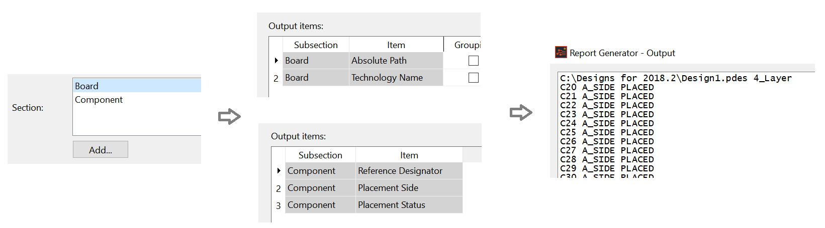
For each element of a PCB that you select in the Section box, the Output items table allows you to configure the attributes that you add from the Available items box. For each attribute, you can specify its position for each section in the report, and whether the data is sorted on it. You can also specify the sort priority, grouping, column width and alignment values that are applied when the report is generated. The attributes are reported on by section first, and then in the order specified in the Output items table. For example, if Board and Component are displayed, in this order, in the Section box, and the attributes are displayed in the order shown below, then the report is generated as shown.
| Value | Description | |
|---|---|---|
| Subsection | Displays the item that you select in the Section box. This is the element of a PCB for which the attribute in the Item column is associated. | |
| Item | Displays the attribute that you select in the Available items table. If you add any attributes related to Component symbol or Component strings to the Output items table, then the Layer name field is displayed in the Item settings section. If you add the User attribute item to the Output items table, then the User attribute name box is displayed in the Item settings section. This allows you to select the required layer, system or user attribute, or 3D model that is associated with the relevant attribute. | |
| Sort | The Sort column allows you
to sort the data for a relevant attribute in ascending or descending
order. Data can be sorted on more than one attribute. For example,
the following data is sorted first on ascending Part
Name value, and is then sorted on ascending Reference
Designator value. This means that the part "FID100X300" is listed after
the part "CSD16323Q3",
and the reference designators "FID1"
, "FID2" and "FID3" are listed in ascending
order for this part.
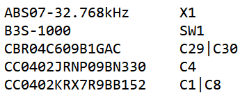
CSD16323Q3 IC2 CSD16323Q3 IC3 FID100X300 FID1 FID100X300 FID2 FID100X300 FID3 GRM0332C1H100GA01D C10 GRM0332C1H100GA01D C11 The Sort column is displayed if you select Sort in the Format options section.Note
|
|
| None | The data is not sorted on the relevant attribute. | |
| Ascending | The data is sorted in ascending order, alphanumerically. As
the sorting is done using natural ordering, "C2" is
displayed before "C11", as shown below.
C1 C2 C3 C4 C10 C11 |
|
| Descending | The data is sorted in ascending order, alphanumerically. As
the sorting is done using natural ordering, "C2" is
displayed after "C11", as shown below.
C11 C10 C4 C3 C2 C1 |
|
| Ascending (String) | The data is sorted in ascending order, alphanumerically. The
order of the data is defined using the alphanumeric position of
each individual character. This means that "C11" is
listed before "C2", as shown below.
C1 C10 C11 C2 C3 C4 |
|
| Descending (String) | The data is sorted in descending order, alphanumerically. The
order of the data is defined using the alphanumeric position of
each individual character. This means that "C2" is listed
before "C11", as shown below.
C4 C3 C2 C11 C10 C1 |
|
| Sort priority | Allows you to specify the order in which the displayed attributes
are sorted. An attribute item with a smaller Sort
priority value is prioritized over attributes with larger
values. Specify an integer that is greater than or equal to "1".
For example, the following data, which is grouped on Part
Name value, is sorted first on ascending Part
Name value, (Sort priority
"1"), and then on ascending Reference
Designator value (Sort priority
"2"). This results in the data being displayed in order
of ascending Part Name value,
with the Reference Designator values
listed in ascending order, as shown below.
|
|
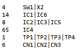
| Grouping | For an attribute for which Grouping
is selected, this setting allows you to display items on the same
row that have identical values. You can select Grouping
for multiple attributes. The following example shows a report
that is grouped on Pin Count.
The Reference Designator values
that have the same value for Pin Count
are displayed on the same row.
Note
|
|
| Selected | Items that have identical values for the relevant attribute are displayed on the same row. | |
| Not selected | Attributes are displayed on a separate row for each component. | |
| Width | Allows you to set the width of a relevant column in the report
by specifying the number of characters. This column is displayed
if you select Specify width in
the Format options section. Specify
an integer that is greater than or equal to "1".
Note
|
|
| Alignment | Allows you to specify whether an attribute is aligned to the left or right of the relevant column in the report. The attribute is aligned by adding the required number of spaces. For example, if a value with one character is aligned to the right of a column of width "20", then 19 spaces are added before it. This field is displayed if you select Specify width in the Format options section. | |
| Left | The attribute in the relevant column in the report is aligned to the left by adding the required number of spaces to the right of it. | |
| Right | The attribute in the relevant column in the report is aligned to the right by adding the required number of spaces to the left of it. | |

|
The item that you select in the Output items table is moved to the top of the table. In the generated report, this attribute is displayed at the top of the section that is selected in the Section box. | |
|
|
The item that you select in the Output items table is moved up one row in the table. In the generated report, this attribute is displayed in the specified position in the section that is selected in the Section box. | |
|
|
item that you select in the Output items table is moved down one row in the table. In the generated report, this attribute is displayed in the specified position in the section that is selected in the Section box. | |

|
The item that you select in the Output items table is moved to the bottom of the table. In the generated report, this attribute is displayed at the bottom of the section that is selected in the Section box. | |
| Delete | Deletes the item that you select in the Output items table. Alternatively, right-click it and then choose Delete Selected Rows on the assist menu. You can select multiple items using the Ctrl or Shift key, or by dragging the cursor in the Output items table. |
Item settings
This section allows you to select a value for the required layer or user attribute, or specify a string. This section is blank unless the items specified below are selected.
| Item | Description | |
|---|---|---|
| Layer name | This field is made available if you add any attributes related
to Component symbol or Component strings to the Output
items table. If you add Component
symbol, Component symbol coordinates,
Component symbol coordinate X or
Component symbol coordinate Y to the Output
items table, then the following layers, on which component
symbols can be added, can be selected.
If you add Component strings, Component strings coordinates, Component strings coordinate X or Component strings coordinate Y to the Output items table, then any symbol layer or user-defined layer can be selected. For the specified layer, component symbols are shown in the Report box. |
|
| User attribute name | This field is made available if you add User
attribute to the Output items
table.
|
|
| Text | Allows you to specify any text or symbol. The specified content
is shown for each row in the Report box,
in the position specified in the Output items
table. The Text field is displayed
if you add Text to the Output
items table by selecting it in the Available
items section, and then clicking |
Format options
| Item | Description | |
|---|---|---|
| Sort | Selected | Displays the Sort and Sort priority columns in the Output items table. The Sort column allows you to sort the data for a relevant attribute in ascending or descending order. Data can be sorted on more than one attribute. When multiple attributes are displayed in the Output items table, the Sort priority column allows you to specify the order in which they are sorted. An attribute item with a smaller value is prioritized over attributes with larger values. |
| Not selected | The Sort and Sort priority columns are not displayed in the Output items table. | |
| Grouping | Selected | Displays the Grouping column in the Output items table. For an attribute for which Grouping is selected, this setting allows you to display items on the same row that have identical values. You can select Grouping for multiple attributes. |
| Not selected | The Grouping column is not displayed in the Output items table. | |
| Specify width | Selected | The Width and Alignment columns are displayed in the Output items table. The Width column allows you to set the width of a relevant column in the report by specifying the number of characters. If you specify a value that is less than the width of an attribute value, then the value is truncated. The Alignment column allows you to specify whether the content in a relevant column in the report is aligned to the left or right, by adding spaces to it. |
| Not selected | The Width and Alignment columns are not displayed in the Output items table. The columns in the generated report are separated by a single space. |
| Value | Description | |
|---|---|---|
| Variant | If the current design contains variants, then the Variant
field is made available. This allows you to either select Master, or a variant that exists in the design.
Note
|
|
| Master | If selected, then the generated report contains information for all components in the design. | |
| [Variant] | If a variant in the design is selected, then the generated report contains only information for the components in the selected variant. | |
| View | Generates a report that is based on the settings in the
Report Generator dialog. This is
displayed in the Report box at the
bottom of the dialog. The generated data is not saved automatically,
but can be saved by clicking Save as.
After you generate a report by clicking View,
you can then display the generated data in a pop-out report window
by clicking . |
Report
| Item | Description |
|---|---|
| Report box | When you click View, the
data is displayed that is generated using the settings in
the Report Generator dialog. You
can display this data in a pop-out window by clicking . This data is not saved
automatically, but can be saved by clicking Save
as. You can change the height of the report box by dragging
the divider shown below.
|
|
|
Displays the Report Generator
Output dialog. This is a pop-out dialog which allows you to
more-easily view the contents of the generated report, and save
them as a .txt or .csv
file. Clicking displays the data that was previously
created by clicking View. It
does not actually generate the data. |
| Save as | Allows you to save the generated data by specifying the extension of the exported file. You can select either .txt
or .csv in the displayed Save As dialog. The contents of the file are identical, regardless of the selected file extension. This data is not saved
automatically when you generate a report. See: Supported
CSV Format.
Note
|
| Close | Closes the Report Generator dialog. If you make changes in the dialog, then a confirmation dialog is displayed which prompts you to save them. |
You can zoom the display in the Report box and the Report Generator Output dialog by pressing the Ctrl key and scrolling the mouse wheel.
