
The following procedures describe how to create a star point, and move its virtual pads to the required layers. For a single layer, you can create a star point using a pad. For multiple layers, specify a through hole padstack that has multiple, virtual pads. The number of virtual pads defines the maximum number of connections that can be attached to the star point. They do not all need to be connected, if not required.
In the example below, a four- point, through hole star point is created. It has one padstack, which has one electrical pad and three virtual pads. Initially, all the virtual pads are on the same layer. They are moved to the required conductor layer using the using the Move (Layer) command in eCADSTAR PCB Editor.
Create a Footprint
This procedure describes how to create the footprint for a star point. The steps must be followed in the order shown to ensure that pin numbers are allocated to each pad. This is because pin numbers are not allocated to individual pads that have the same origin.
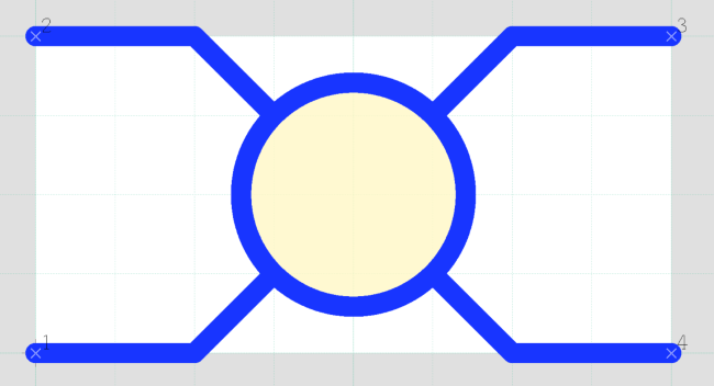
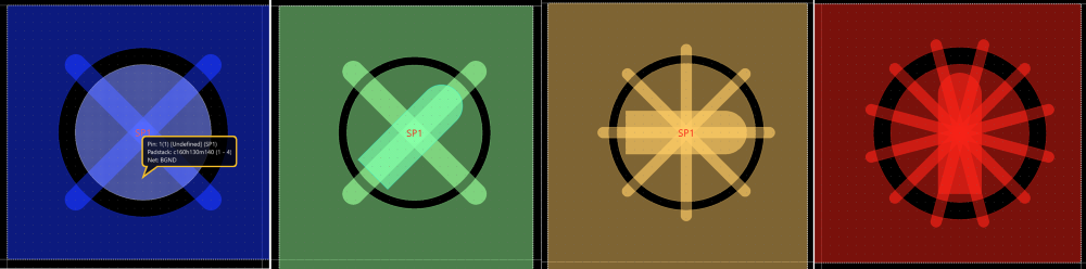
- In Footprint Editor, create a PCB Footprint for the star point. The example shown below has one electrical padstack, shown on the left, and three virtual pads. The virtual pads are defined in the Pad Editor dialog. These have three different placement angles, which makes it easier to select them in eCADSTAR PCB Editor.
- Allocate pin numbers to the padstack and virtual pads. Ensure that pin 1 is allocated to the Padstack.
- Arrange the pads so that their origins are coincident. In the following image, all pads are highlighted to show their positions.
- To specify the footprint as a star point, select the Star point check box in the Footprint Attributes panel.
Create a Schematic Symbol
In Symbol Editor, create a schematic symbol with four pins. These match up with the four pins that are allocated in the footprint. This is illustrated below.
Create a Library Part
- In the Parts tab in eCADSTAR Library Editor, create a new part by clicking Home > Rows > Add.
- Select the part in the Parts tab, and click Home > Edit > Part on the ribbon. The Part Editor is launched.
- In the Detail tab in Part Editor, associate the symbol with the newly-created PCB footprint for the new part.
- In the Part Information section, select the Star Point radio button. This specifies that the part is created as a star point.
You can create a single-layer star point using this process. In this case, all pads are placed on the Top_Elec layer in the Library. This includes both electrical and virtual pads.
Add the Star Point to eCADSTAR PCB Editor
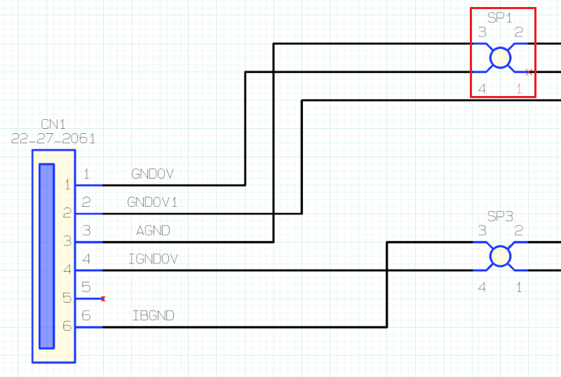
- Add the star point symbol to a schematic in eCADSTAR Schematic Editor. This is illustrated below.
- In eCADSTAR PCB Editor, add the star point using the Forward Annotation command. In the example shown below, all the virtual pads to be connected are on Conductor-1.
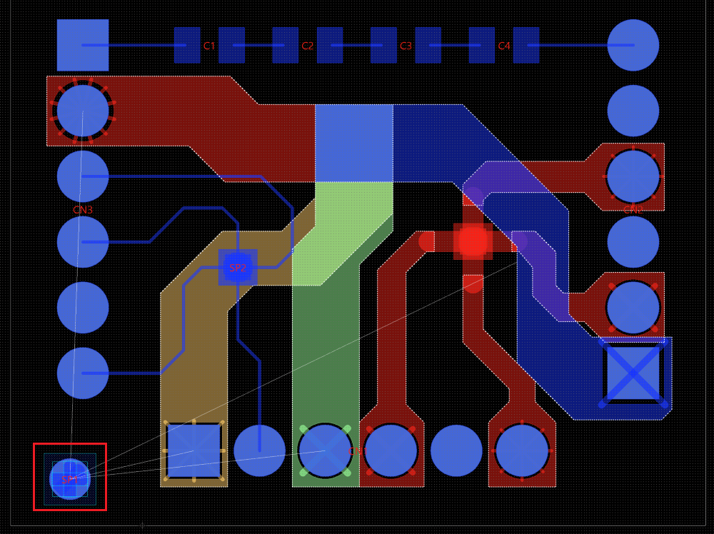
Associate each Virtual Pad to a Layer
- To allow a signal to be connected to each virtual pad in the star point, each one must be moved to the correct layer. Do this by selecting the virtual pad on the canvas in eCADSTAR PCB Editor, and clicking Home >Move > Layer on the eCADSTAR PCB Editor ribbon. The Move (Layer) dialog is displayed.
You can scroll through selected items that are placed on top of each other by pressing the N key.
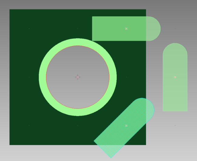
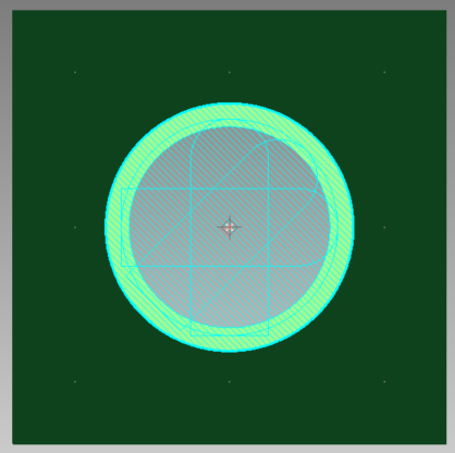
- In the Layer Settings panel, make each relevant layer visible, individually. The virtual pad that is placed on that layer is displayed. The following image shows planes that are flooded on each layer into the star point.
The following recommendations are provided for creating star points.
- For a star point on a single layer, all pads must be connected or DRC errors are generated. Redundant pads can be connected to an existing net on the star point.
- Keep virtual pads inside the padstack.
- Because padstacks cannot be moved to inner layers, do not use them to create a single-layer star point.
