
Appendix J: Post Processing a Part with Common Pins
Parts with common pins within the CADSTAR libraries require a post processing task to support the data structure of eCADSTAR. The following actions must be followed in eCADSTAR
- Modify the footprint used for the part with common pins.
- Modify the part with the common pins.
- Reload into the schematic design.
- Forward annotate to the PCB design.
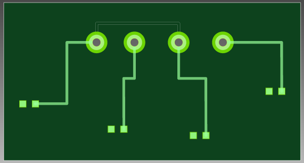
In the following example, the schematic design has a symbol with 3 pins defined for component CP1. The PCB design has 4 through hole pins defined for the component CP1. Pins 1 and 3 have been connected using component copper on a non-electrical layer within CADSTAR.
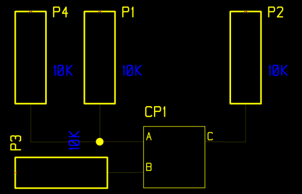
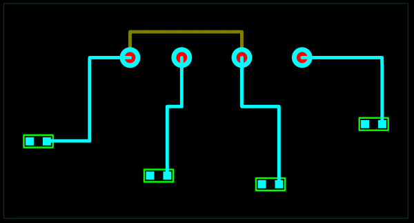
Figure 1: CADSTAR schematic and PCB designs with a part using common pins
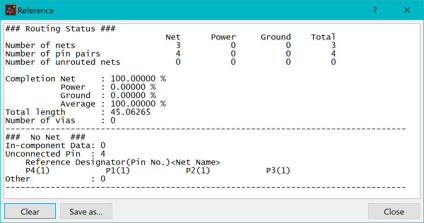
After the designs are migrated to eCADSTAR, the PCB design shows a net connection between the two common pins and also now indicates the design is not 100% routed.
Figure 2: Resulting migration of the PCB design in eCADSTAR
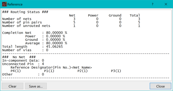
Figure 3: Routing report of the migrated design in eCADSTAR
The following process should be followed to address this difference in the support of parts with common pins.
Modifying the Footprint Used for the Part with Common Pins
- Open the master library that contains the part with common pins, and identify the part within the eCADSTAR Library Editor grid.
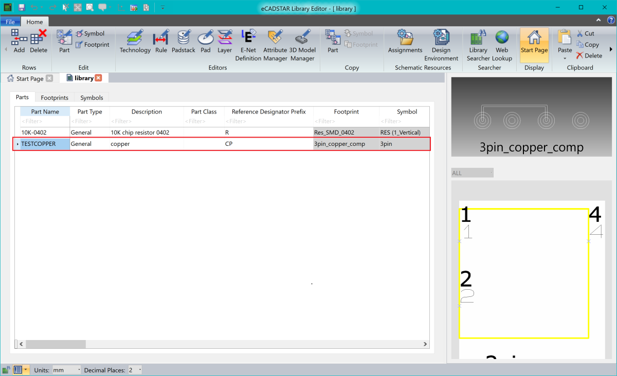
Figure 4: Part Editor showing the part with common pins
- With the part row selected, click Home > Edit > Footprint on the ribbon, or use the option on the assist menu.
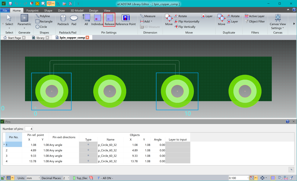
Figure 5: Footprint Editor with the Common Pin Footprint highlighted
- On the ribbon, click Home > Pin Settings > Release.
- Select the two padstacks that were connected by the component copper in CADSTAR.
- Click Yes to confirm that the pin number should be released. The assigned pin numbers are released from the padstacks.
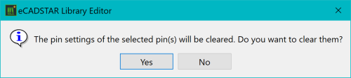
Figure 6: Release pin setting confirmation dialog.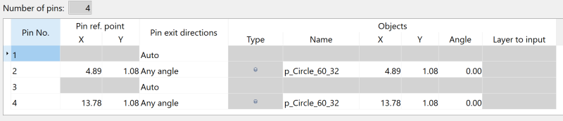
Figure 7: Pins showing unassigned pin numbers.
- Ensuring there is nothing selected on the canvas, click Home > Pin Settings > Individual on the ribbon. ‘1’ should be added to the cursor.
- Press and hold the Ctrl key, and click the two padstacks whose assigned pin numbers were previously released.
If the component copper is present on an electrical conductor layer and is still required on this layer, then the component copper shape should also be assigned the pin number.
- When selected, release the Ctrl key and press the Space bar. The two padstacks are assigned the number ‘1’, and both pins are considered internally connected.
- Exit the Pin Settings (Individual) command.
- In the pins table, select the row with the unassigned pin number and click Delete Pins.
- Click Yes to confirm the deletion of the pin number row.
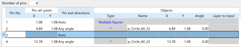
Figure 8: Pins showing the highlighted unassigned pin.
- Save and close Footprint Editor.
Modifying the Part with the Common Pins
- In eCADSTAR Library Editor, select the common pin part row and click Home > Edit > Part on the ribbon. Alternatively, use the option on the assist menu.
Pin 3 in the Pin Assignment table is marked in red.
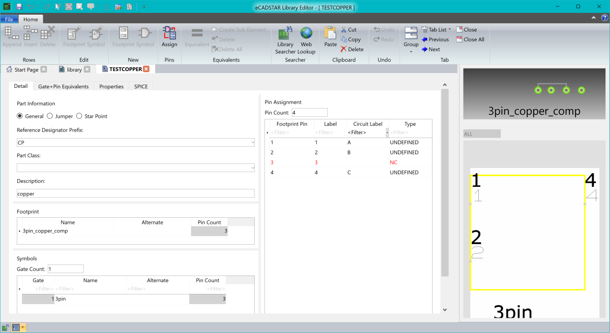
Figure 9: Part editor with highlighted Pin Assignment table
- Select the row for Footprint Pin 3 in the Pin Assignment table, and select Delete Row on the assist menu.
- Select Save and close the Part Editor panel.
Reloading into the Schematic Design
- Launch eCADSTAR Schematic Editor, and open the schematic design that contains the part with common pins.
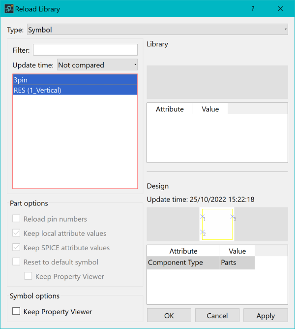
- Click Component > Library > Reload on the ribbon to launch the Reload Library dialog.
- In the Type box, select Symbol.
- Select all symbols in the list and click Apply. The symbols are reloaded to match the master library.
This is an advisory step to ensure that the design library symbol matches the master library symbol.
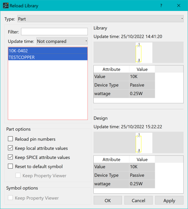
- In the Type box, select Part.
- Select all parts in the list and click Apply. The parts are reloaded to match the master library.
- Close the Reload Library dialog.
- Save the design and exit eCADSTAR Schematic Editor.
Forward Annotating to the PCB Design
- Launch eCADSTAR PCB Editor.
- Open the PCB design which is associated with the updated schematic that contains the part with common pins.
- Click Design > Design Changes > Forward Annotation on the ribbon.
- Select the schematic design which was previously updated by the Reload Library process.
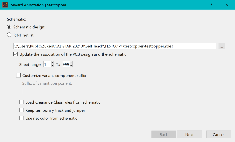
- Click Next, and then click Finish.
- Click Yes to proceed with the forward annotation.
- Close any report dialogs that appear.
On completion, the remaining net connection should be minimized from the design.
- The routing completion report now indicates that the design is 100% routed. The design data is now aligned, and uses the eCADSTAR method for supporting common pins.
Appendix A: File Types
Appendix B: Determining the Input Data
Appendix C: Cadstar Layer Sub Types
Appendix D: Global Signals
Appendix E: Mapping Recommendations
Appendix F: High Speed Migration
Appendix G: Migration of Padstacks
Appendix H: Post Processing a PCB Design that is Annotated using a RINF Netlist
Appendix K: Additional Notes
