
Appendix F: High Speed Migration
High Speed Migration: Preparing CADSTAR files
Before executing the CADSTAR to eCADSTAR migration, ctf files must be created for the schematic and PCB data. To ensure that the correct ctf files are created, follow the steps below.
For a schematic:
- Open the schematic design data and launch Constraint Browser. This is done in CADSTAR by clicking Tools on the ribbon, and then clicking Constraint Browser.
- Ensure that all constraints are set in Constraint Browser, and click Save. This will then create a sub directory in the directory in which the design data is saved. The sub-directory should display the same name as the schematic CSA design file. This is demonstrated in the following example.
- A sub-directory with the same name as the schematic ASCII is found, and a schematic ctf file is found within this sub-directory "[Schematic CSA name]\hotstage\data\[Schematic CSA name].ctf". For example, "test\hotstage\data\test.ctf".
If the design is used in Legacy Constraint mode in CADSTAR, then the schematic-based CTF file must be generated by executing the Back Annotation command for the PCB design.
For a PCB:
- Open the PCB design data and open Constraint Manager. This is done in CADSTAR by clicking Tools on the ribbon, and then PREditor XR HS. Ensure all constraints are set within Constraint Manager and click Save. This will then create a sub directory within the directory in which the design data is saved. The sub-directory should display the same name as the PCB cpa design file. This is demonstrated in the following example.
- A sub-directory of the same name as the PCB ASCII is found, and a PCB ctf file is found within this sub-directory "[PCB cpa name]\hotstage\data\[PCB cpa name]\[PCB cpa name].ctf". For example, "test\hotstage\data\test\test.ctf".
When these ctf files have been created, the High Speed migration process can start.
High Speed Migration Steps
Follow the same migration steps as described for non High Speed designs, in this guide. These steps describe how to create schematic and pcb archive files. All pre-migration steps must be followed that are described in the Migrating CADSTAR to eCADSTAR: Getting Started topic. Then, continue with the High Speed migration process.
- Ensure that the ctf files are in a sub directory within the same directory as the .cpa and .csa design data. In order to migrate the High Speed data, the ctf files must have the same file name as the corresponding .cpa and .csa files.
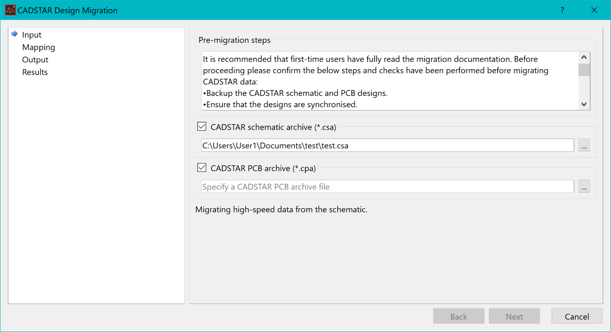
- To start the migration process, specify the schematic design data (the .csa file in the migration wizard).
- If the ctf file is found in the directory, then the message "Migrating high-speed data from the schematic" is displayed. This is illustrated below.
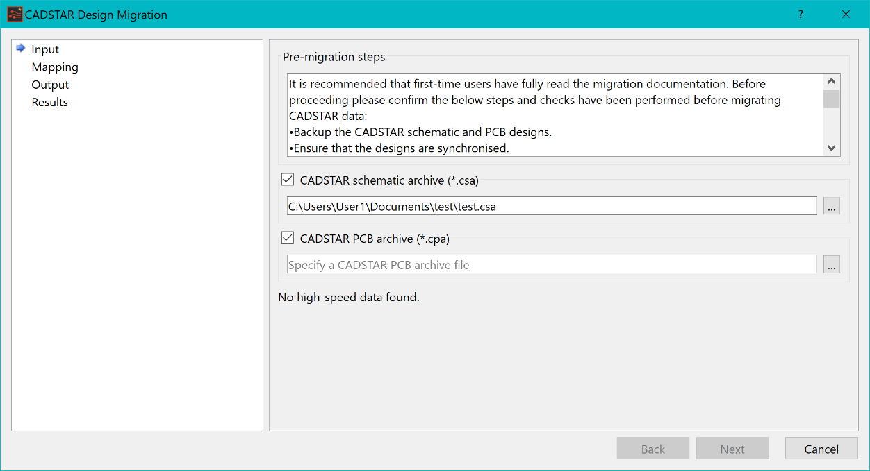
- If the message states that no High Speed migration data is found, then check the directory structure to ensure it is as described above. This is illustrated below.
High Speed schematics cannot be migrated on their own, and therefore need a PCB cpa file to be specified. To migrate only a schematic design, the ctf file must be removed from the directory.
The procedure to specify a PCB cpa file is described below.
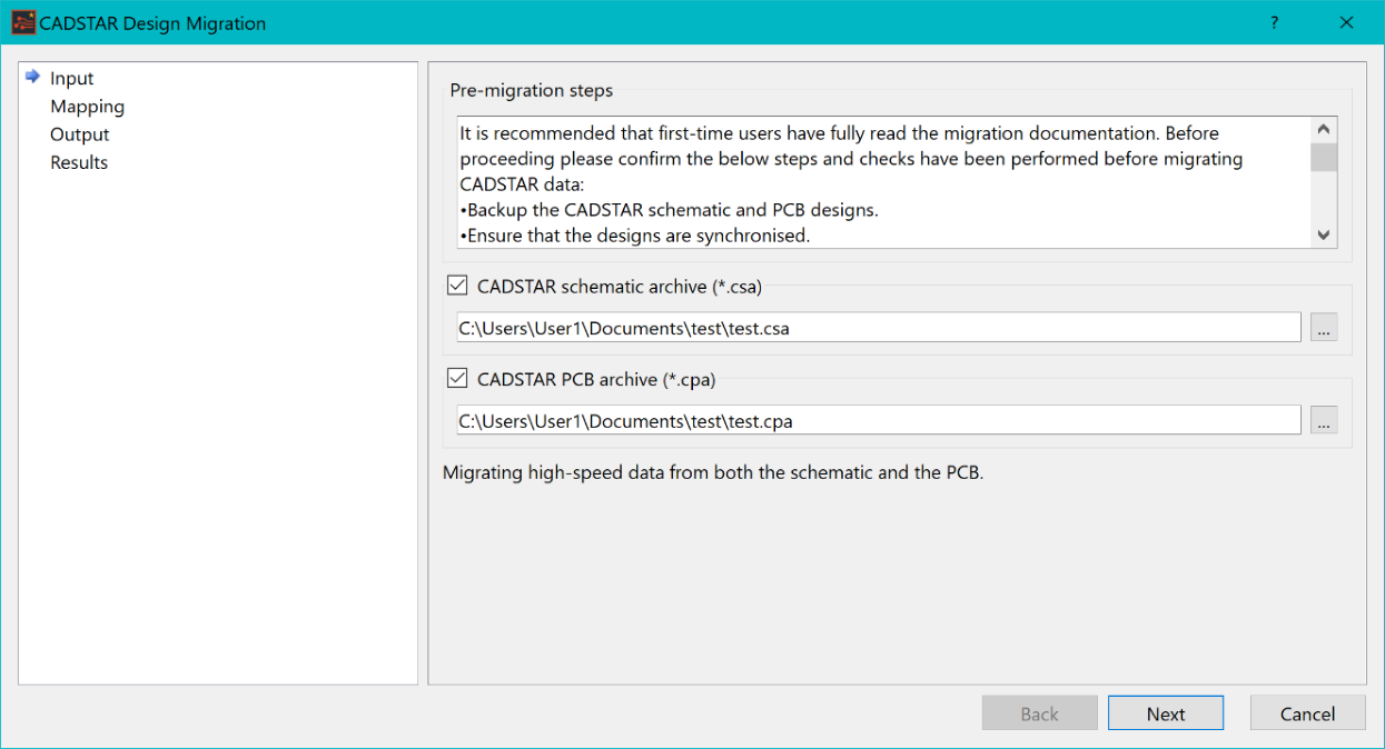
- Using similar methods to those described above, browse to a PCB archive file.
- If High Speed data is found, and the ctf file exists in the correct directory structure, then the dialog indicates that High speed data will be migrated. This is illustrated below.
- If no data is found, then a message is displayed in the dialog to indicate this.
- Click Next, and continue with the migration process as outlined in the standard migration steps. This includes specifying a mapping file, and choosing an empty output directory. When you have completed these sections of the wizard, proceed with the migration process.
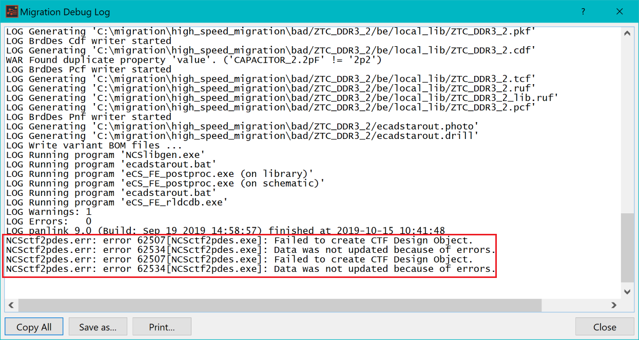
- Errors that are found during the migration process are shown in the panlink file. These are shown after the line that states the migration process has finished. This is illustrated below.
Appendix A: File Types
Appendix B: Determining the Input Data
Appendix C: Cadstar Layer Sub Types
Appendix D: Global Signals
Appendix E: Mapping Recommendations
Appendix G: Migration of Padstacks
Appendix H: Post Processing a PCB Design that is Annotated using a RINF Netlist
Appendix J: Post Processing a Part with Common Pins
Appendix K: Additional Notes
