
CADSTAR PCB Component Library Preparation
This topic provides recommendations for preparing your CADSTAR PCB Component Library data for migration. For CADSTAR, the library-to-template layer mappings are considered to be "one-to-one", based on layer names. This allows the eCADSTAR PCB Editor Component Library Layers to be defined with a minimum of one electrical layer.
For eCADSTAR, the library-to-technology layer mappings are not considered to be mapped on a one-to-one basis. You must define the library layer mapping to the design technology layers. However, the library layer-to-technology layer mapping can map a single library layer to many technology layers. Further information on library-to-technology layer mapping is available in the following topics.
Data Preparation of CADSTAR Template Designs
Migrating the CADSTAR Template Data
Finalizing the Template (Technology) Migration
Finalizing the Template (Design Rule) Migration
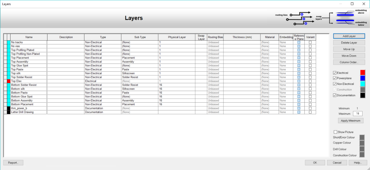
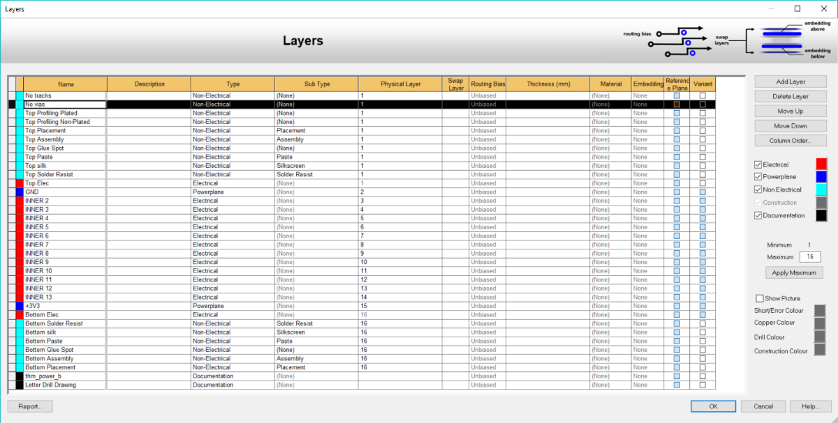
To improve post-migration tasks and reduce long-term library management and maintenance, it is recommended to set the CADSTAR library layers to the following four layers.
- Top Electrical
- Inner
- Inner Suppressed
- Bottom Electrical
This approach minimizes the work required to manage the eCADSTAR library, and allows a single library to be easily used with multiple technologies. A single inner layer can be mapped to all required inner layers. If a pad needs to be modified, then only the single definition for the inner pad needs to be changed.
The design can be quickly changed to use pad suppression by modifying this technology page. Define the usage of the Inner Suppressed definition for the inner layers.
For further information on configuring pad suppression, see: Finalizing the Padstack "Inner Suppressed" update.
The above method for CADSTAR library migration has the disadvantage of not allowing the control of shape or size reassignments on specific internal layers for any pad definition.
If using a complete layer stack within the eCADSTAR PCB Editor Component Library, then this can be suitably migrated to eCADSTAR. However, this will greatly increase the process of Library management and maintenance in eCADSTAR. This is the result of how eCADSTAR creates, stores and maps padstack definitions from the library into the PCB design.
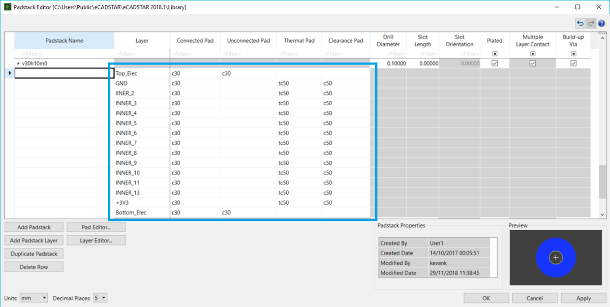
In this example, the CADSTAR Library has 16 electrical layers. The migration process can create 16 conductor layers within the resulting eCADSTAR library. Padstacks defined in the eCADSTAR library will require a pad shape to be mapped to each of these 16-conductor layer. Because there is no concept of a ‘Default’ pad shape and size, and specific layers use re-assignments to obtain different pads on specific layers.
Pad shape definition in a padstack item is required on each Library conductor layer, and is defined for "Connected", "Unconnected", "Thermal" and "Clearance" pads within the eCADSTAR Library. Therefore, management and maintenance tasks are increased when creating or modifying padstack items. It is recommended to minimize the CADSTAR Library Layers for electrical layers, as detailed earlier. In the example of 16 conductor layers, the padstack definitions may require up to 64 pads to be assigned against all the conductor layers. This will represent a large set of actions when creating a new padstack.
An additional library maintenance cost is incurred when the eCADSTAR library layer count is increased. In this example, if 16 layers are increased to 18 layers, then every padstack definition would need to be manually edited to add pad assignment to each of the two new layers. If the library contained 250 padstack definitions, then ten steps would be required against each padstack definition. This represents a task of 2500 actions to update the library.
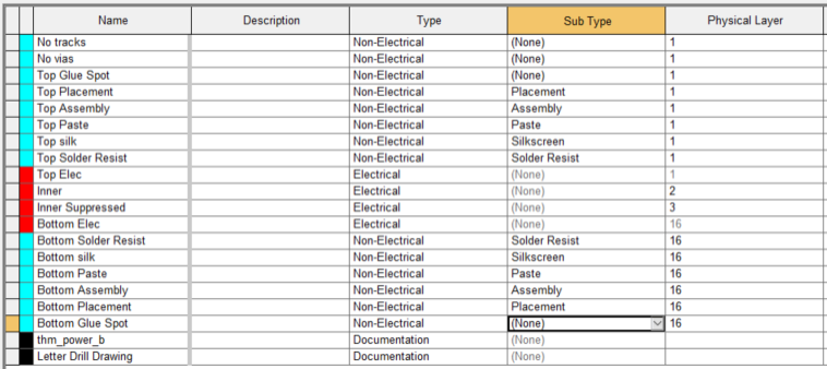
To enable a simpler migration of CADSTAR Library to eCADSTAR, it is recommended to set up the layer "Sub Type" for the Placement, Assembly, Paste, Silkscreen and Solder Resist layers before proceeding with the migration.
Only one Sub Type should be applied in the CADSTAR library. If the multiple layer Sub Type is set for multiple layers, then data from CADSTAR is merged into a single layer in the resulting eCADSTAR Library. For example, where a second silkscreen is defined, this should be set with a layer Sub Type of (None). This layer must then map to a separate layer in eCADSTAR. For details on mapping content from CADSTAR to eCADSTAR , see: "Setting up CADSTAR to eCADSTAR Mapping Options".

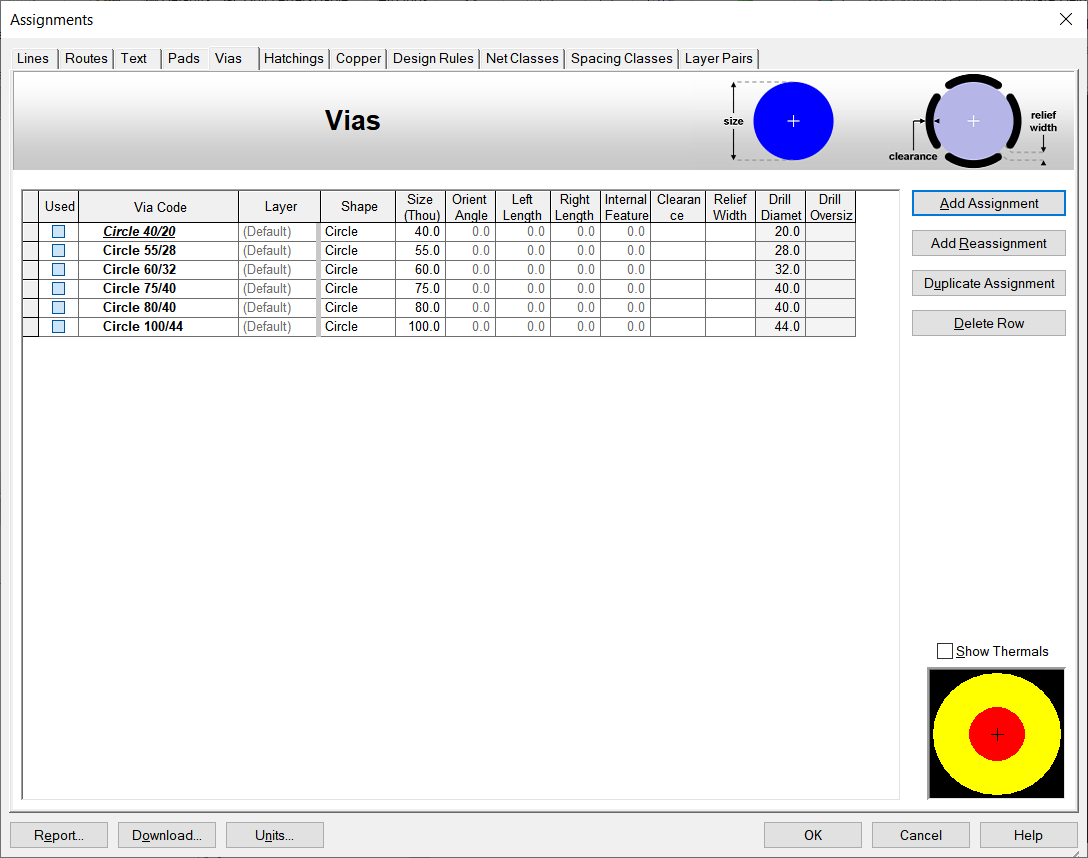
There are significant differences between CADSTAR and eCADSTAR in the definitions of padstacks for vias. Within CADSTAR, the Pad definitions for vias are solely defined within the design, or the initial template that is used for a design. However, in eCADSTAR, the padstack via definitions are based in the library, with all the padstacks defined for component pads.
To ensure the ease of post migration tasks for eCADSTAR Library and Design alignment, it is recommended that the template and design via definitions are added into the CADSTAR Library assignments before library migration is performed. Prefix assignment names with "v " to indicate the usage of the pad definition as a via.
The via definitions contained in all the PCB template designs should be added into the CADSTAR library Pad Assignments. This ensures that the best migration results are achieved.
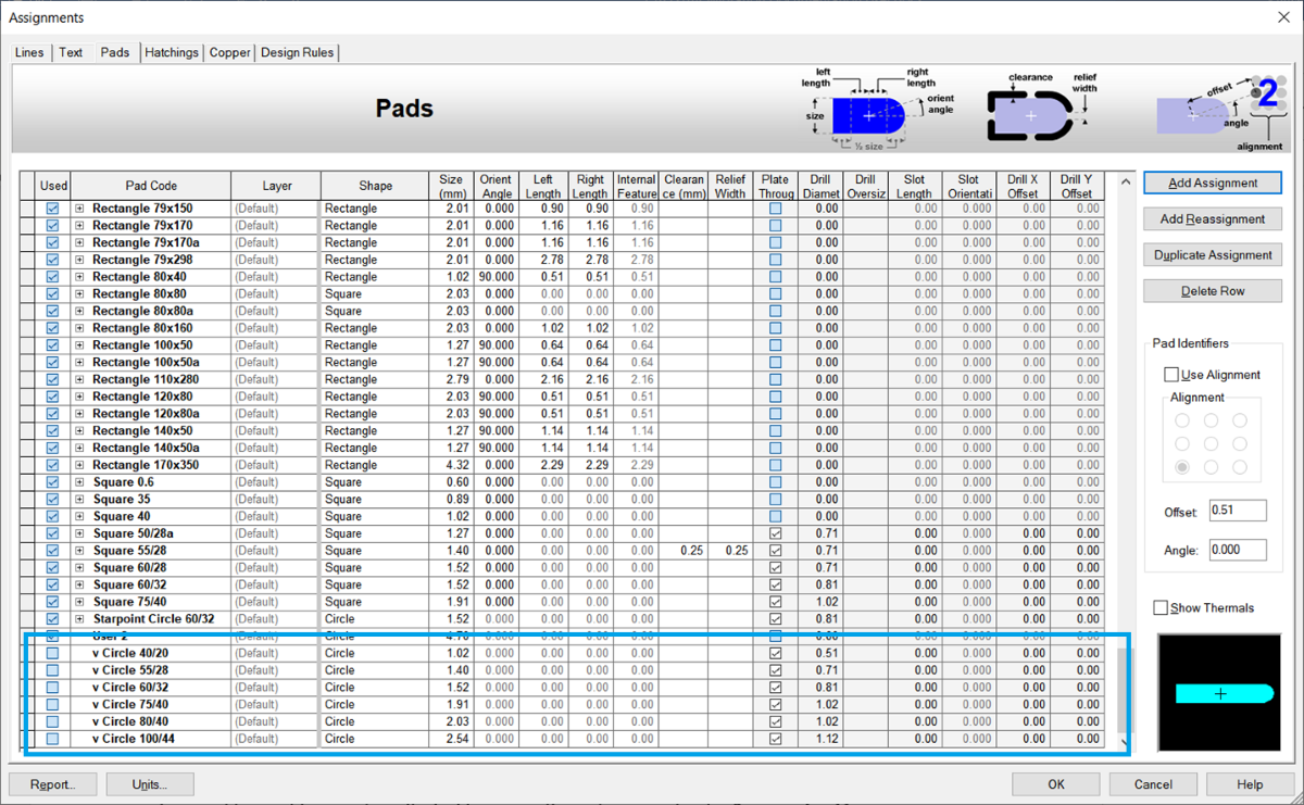
Adding new Pad definitions into the CADSTAR PCB Library
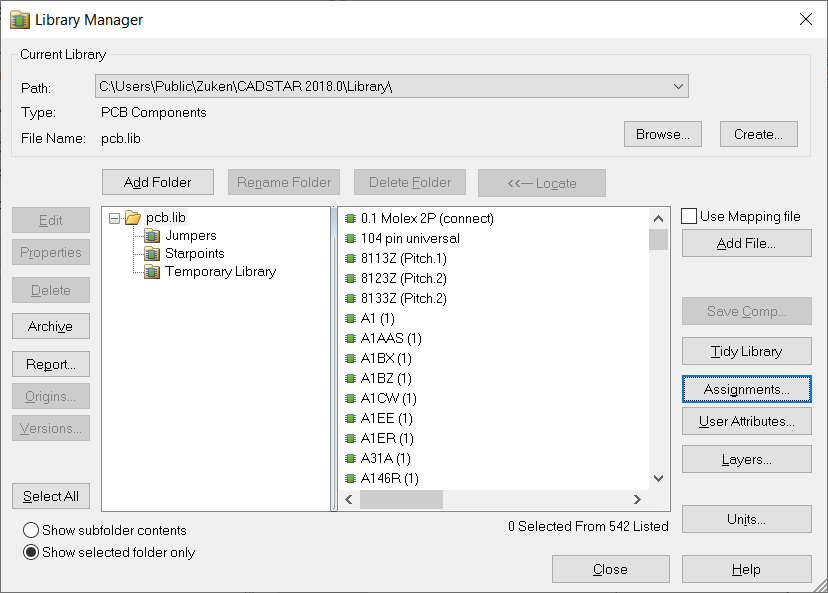
- Launch CADSTAR Library Editor application, and ensure that the selected library is: C:\Users\Public\Zuken\CADSTAR 2018.0\Library.
- In the Library tab, Manage group, select PCB Components.
- Click the Assignments button. The Assignments dialog is displayed.
- Select the Pads tab to display the defined pads grid.
- Select a row in the grid and click Add Assignment to add a new row to the grid.
- Enter a via pad name as defined in the template design, and prefix it with the "v". For example, "v Circle 40/20". Set the parameters of the pad definition to be the same as defined in the template design.
- When all via pad definitions are inputted, click OK to apply the changes and close the dialog.
To finalize the PCB Component Library Preparation, output an archive (cpa) file of the full binary library. This is described below.
- Launch CADSTAR Library Editor application.
- In the Library tab, Manage group, select PCB Component.
- In the Library Manager dialog, select the top level (.lib) item in the left-hand list.
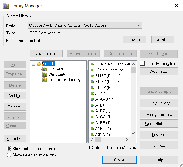
- Click the Archive button.
- In the Export to File dialog, click the Browse button.
- Select the migration directory that is defined during the preparation of the part library data for migration.
- Click Save to apply the settings and close the dialog.
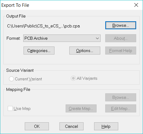
- Click OK to export the entire content of the PCB Component binary library to the archive file format (cpa).
- Locate the exported archive file into the prepared library directory for the migration. Data preparation for the CADSTAR PCB Component library is now complete.
To export a subset of the PCB Component library, a selection can be made in the component list. When Archive is now executed, the selection is exported to the cpa file.
