
The contents of the Via hole sub-tab in the Conductor Clearance tab of the Rule Editor dialog are described below. This sub-tab allows you to optionally specify minimum clearances for via holes. This is done by specifying a value in the cell where the Clearance type row intersects with a column that represents the relevant net and layer configuration.
| Item | Description | |
|---|---|---|
| Clearance Priority | Allows you to select how the effective value for conductor clearance is set. This can be set by searching a hierarchical list of clearance values. Clearance rules that are set in the Conductor Clearance: Voltage Difference Tab, Constraint Browser or the Default Design Rule Stack section in Rule Editor are followed, in the hierarchical order shown below. Alternatively, you can specify that the largest clearance value is used that is set in either Constraint Browser or Rule Editor. | |
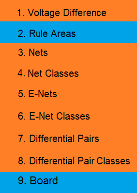
| Use hierarchy | The effective value for conductor clearance is set by checking
clearance rules in the following order. The first clearance value
that is found is used. Click the rows in the following image for
a description of where the relevant values are set.
Note
|
|
| Use largest value |
The largest clearance value is used that is set in either the Design Rule sub-tab, Voltage Difference Clearance section in Constraint Browser, or in the Default design rule stack section in Rule Editor. In the following example, a clearance of 0.1 mm is set in the Default design rule stack, and a clearance formula of 0.00305 * Vdiff + 0.05000 is specified in the Clearance dialog.
Below approximately 16V, the clearance is defined by the Default design rule stack. Above this voltage, the clearance is defined by the formula as this produces the largest clearance values. |
Clearance Type Settings
Clearances between types of via hole are described below. Clearances for build-up via holes can be specified for via holes in the same net, or in different nets. They can also be specified on the same layer, or on different layers.
You can add the same value to the whole table as follows:
- Press Ctrl+C to copy a value from the relevant cell in the Design Rule group table.
- Select all cells in the table.
- Press Ctrl+V to paste the copied value into all cells.
