The Clearance dialog allows you to select a clearance value for a particular voltage range in the Conductor Clearance: Voltage Difference tab, in the Rule Editor dialog. The clearance values are set in the Design rule group section of the Conductor Clearance: Conductor tab in the Rule Editor dialog. It also allows you to specify a formula for calculating clearance. If specified, then this is displayed in the Clearance column in the Voltage Difference tab, rather than a clearance value.
Launch the Clearance dialog
by pointing the cursor in the Clearance column in the Voltage
Difference tab, and clicking the displayed  button. Clearance values are checked using the Creepage
Check command. The results are displayed in the Creepage
Check Results dialog.
button. Clearance values are checked using the Creepage
Check command. The results are displayed in the Creepage
Check Results dialog.
Clearance rules can also be set in Constraint Browser or the Default Design Rule Stack section in Rule Editor. The effective values for conductor clearance are set in the Clearance Priority section of the Rule Editor dialog. This defines the creepage values that are checked by the Creepage Check command.
| Item | Description | |
|---|---|---|
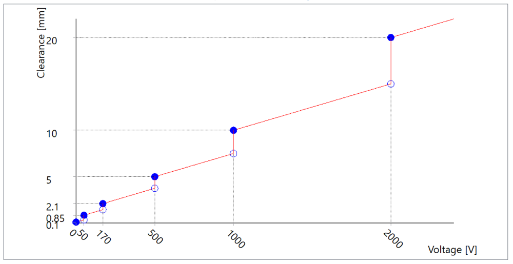
| Formula tab | Allows you to specify a formula for the relevant clearance,
rather than a clearance value. The specified formula is displayed
in the Clearance column,
in the Voltage Difference
tab, rather than a clearance value. If you specify clearances
using a formula, then the clearance value increases relative to
voltage for each threshold. The minimum clearance is used as a
start point. This is illustrated below.
|
|
| Formula box | The conductivity and vulnerability to creepage of a board is
affected both by the material that comprises it, and its working
environment. At a sufficient voltage, creepage occurs when the
insulator (FR4) breaks down and becomes a conductor. It is also
more likely to occur when levels of moisture or pressure are high.
For this reason, the Formula box allows
you to calculate the clearance value using the following linear
algorithm, which is based on typical conditions:[Coefficient]*Vdiff+/-[Offset].
This formula is used in the Voltage
Difference tab instead of a clearance value. The specified
formula determines the effective clearance, by considering weighting
for the material of the board, and its environment.
|
|
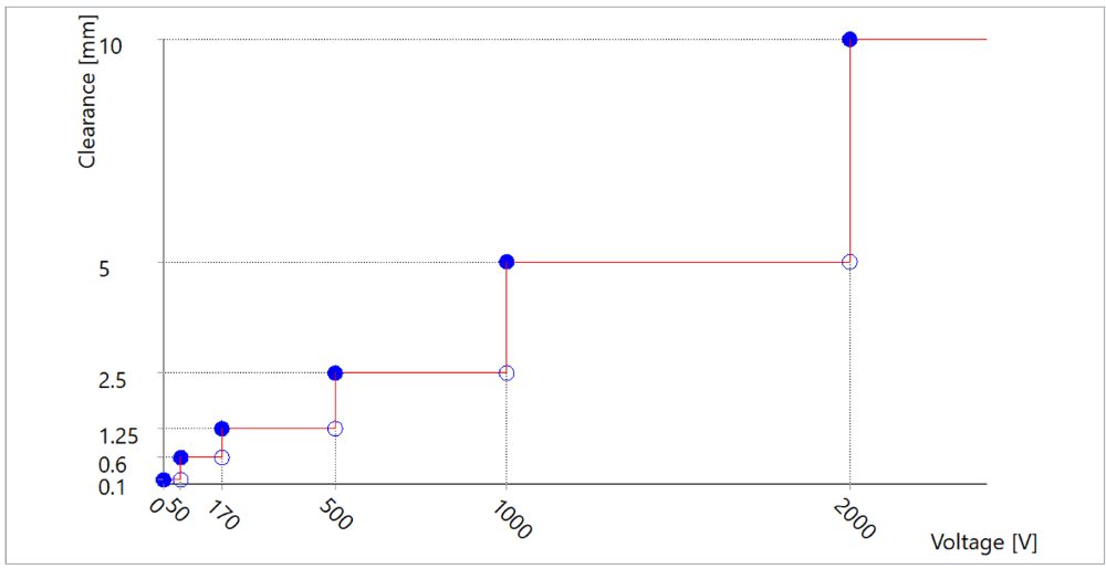
| Design Rule Group tab | Allows you to select a clearance value that is specified in
the Design rule group section
of the Conductor
Clearance: Conductor tab in the Rule
Editor dialog. If you specify clearances using clearance rules,
then the minimum clearance is displayed that is set for each voltage
threshold in the Voltage
Difference tab, Clearance/Voltage
graph. This is illustrated below.
|
|
| Filter box | Allows you to filter the clearance values that are shown in the Clearance list by entering an alphanumeric value. Items are displayed that contain the specified value. | |
| Clearance list | Displays the clearance values that are specified in the Design rule group section of the Conductor Clearance: Conductor tab in the Rule Editor dialog. Double-click a clearance value to add it to the Clearance column in the Voltage Difference tab, in the Rule Editor dialog. Alternatively, select an item and click OK. | |
| OK | The value specified in the Clearance dialog is added to the Clearance column in the Voltage Difference tab, in the Rule Editor dialog, and the Clearance dialog is closed. Alternatively, double-click an item in the Clearance list to close the dialog. | |
| Cancel | Closes the Clearance dialog without updating the Clearance column in the Voltage Difference tab, in the Rule Editor dialog. |