
Whereas clearance is the linear distance between electrical elements in air, creepage is the distance between electrical elements across an insulating material such as the surface of the PCB. In eCADSTAR, creepage takes into account the existence of through-board slots and through-board cutouts in the insulation. This is illustrated below.
- Clearance is indicated by the red arrows below.
![]()
- Creepage is indicated by the red arrows below.
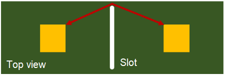
For conductor-to-conductor creepage on a single layer, creepage distance is always greater than or equal to the clearance. As shown above, the creepage distance can be increased by including through-board slots or through-board cutouts in the surface of the PCB. This ensures that the required creepage distances are satisfied within the design. Creepage and clearance distances apply not only to a PCB, but also to components that are mounted on it, particularly magnetic components.
As there are no perfect insulators, creepage should be considered in a design. It is affected by the distance between conductors, as well as the environmental conditions of the insulator. If creepage distances are not maintained for a design, then dielectric breakdown might eventually occur. Tracking might also be compromised. This produces a partially conducting path of localized deterioration on the surface of the insulating material. This is caused by electric discharges on or close to an insulation surface. If clearances are not maintained, arcing might occur.
For a PCB, the insulator is usually the exposed board surface. The effect of creepage is increased with higher voltage differences, and lower resistances. A minimum creepage distance must be maintained which considers these properties, as well as the voltage difference. It is particularly important to consider creepage in the following circumstances.
- When designers are working close to the limits of technologies.
- The high density of components means that meeting only clearance constraints is not sufficient.
- The properties of the PCB are affected by humidity, dirt and other factors.
As working voltage, pollution, overvoltage and altitude increase, both the creepage and clearance distances increase also. Creepage issues occur mostly in high density designs or designs with mixed voltage circuits, such as those for power supplies. The need to check creepage is increasingly important due to the mixing of high and low voltage systems on a single PCB.
Component density has also increased, which reduces the distances between conductors. PCBs are increasingly used in polluted environments, such as automotive, Internet of Things and industrial control. They may also be used in extreme climates. Newer designs are more likely to comprise mixed technologies in which analog, digital and RF circuits are combined closely with high voltage circuits. These require additional isolation rules to ensure operator safety.
By measuring creepage, you are also more likely to meet the regulations for PCB design. These are complex, and can vary between countries. They consider parameters such as working voltages, pollution, operating altitude and overvoltage category. They may also vary between industries, such as medical devices, IT, measurement products, household devices and the military.
In eCADSTAR, clearance rules for creepage are set in the Conductor Clearance: Voltage Difference Tab, Constraint Browser or the Default Design Rule Stack section in Rule Editor. Clearance values are checked using the Creepage Check command, and the results are displayed in the Creepage Check Results dialog. The effective values for conductor clearance are set in the Clearance Priority section of the Rule Editor dialog. This defines the creepage values that are checked by the Creepage Check command.
