
Footprints are objects that represent information on part shapes in PCBs. These are mainly bare-board shapes, but body shape information for 3D parts can also be included. A footprint defines the symbol mark and solder resist figures, and the physical position of component pins, padstacks and other items. A footprint can also be used for non-electrical components such as a company logo and alignment marks. After you have created footprint layers, you can use them to define footprints and padstacks. Padstacks can be placed within footprints, and are described in the Understanding Padstacks topic.
Footprint Layers
Footprints and padstacks reference footprint layers. They do not directly reference layers in your PCB designs. It is important to decide upon an optimum set of footprint layers before you create any footprints, padstacks, etc. Footprint layers are not the same as the layers in your PCB designs. Footprint layers are mapped to real PCB layers in PCB technologies. This means that you can use the same footprints for all your PCB designs, even though they employ many different layer stacks.
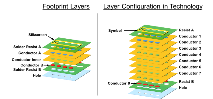
You should define the minimum number of footprint layers that will make the footprints usable for all your designs. For multilayer PCB design, the number of footprint conductor layers is normally far fewer than the maximum number of conductor layers that are used in your PCB designs. The following image illustrates how footprint layers are mapped to real PCB layers.
Note
The single footprint layer Conductor Inner corresponds to six inner PCB layers, Conductor 2 to Conductor 6 in the PCB technology. The same footprint layers can be mapped to different layer stacks with, for example, just two inner layers or even 32 inner layers. The same applies to other footprint layers. You only need to separate footprint layers in cases where padstacks and footprints use them in a unique way.
A separate footprint layer is required for each layer in footprints and padstacks on which you do the following.
- Create figures
- Add text
- Place padstacks
- Place pads
You can create the types of footprint layer shown below.
| Footprint Layer Type | Figures Allowed | Objects Allowed within Figures |
|---|---|---|
| Conductor | Pads within footprints and padstacks, and conductor areas drawn in footprints. | Line, area, pad, text. |
| Solder resist | Solder resist figures. | Line, area, pad, text. |
| Metal mask | Solder paste figures. | Line, area, pad, text. |
| Symbol mark | Ident screen figures. | Line, area, pad, text. |
| Component area | Component area. This can contain a component height restriction. | Component area. |
| Inhibit | Placement or wiring keepout. | Line, area, pad. |
| Hole | Hole figure. | Hole. |
| Non-circular hole (this layer type is used for large and irregularly-shaped holes). | Line, area, pad. | |
| User defined | Layer that corresponds to no other type. For example, a layer on which dimension lines are drawn. | Line, area, pad, text, dimension text. |
