
In the Signal Integrity Analysis environment, a set of relevant Signal Integrity (SI) measurements are performed automatically. These results are stored together with the component information and v(t) and i(t) chart data in the result database file. The Analysis Result Viewer shows these results in the Measurement window, in the Single pin Measurements and Pin-to-Pin measurements tables. A detailed description of the measured results are shown below. The Eye Pattern measurements are described below, including Setup and Hold measurements.
Edge Detection
In order to measure timing characteristics, for example, Flight Time, Slope or Settling Time, which are based on commonly-used definitions, a proper detection of the switching process is required. This identifies individual pulses along the given waveform, and decomposes the waveform into its edges. This is done by checking that particular threshold values are crossed by the signal.
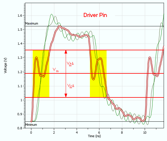
Conditions for the edge detection (Driver)
For waveforms where no suitable thresholds are available, the waveform itself is evaluated. A mean voltage level Vm is calculated as the mean value of Vmax and Vmin. Using thresholds at +/- 25% of the amplitude's swing, an edge is detected.
Vm+ = Vm + D, and Vm- = Vm - D, where D = 0.25* (Vmax - Vmin).
The red colored lines mark these driver's threshold values in the used example waveform.
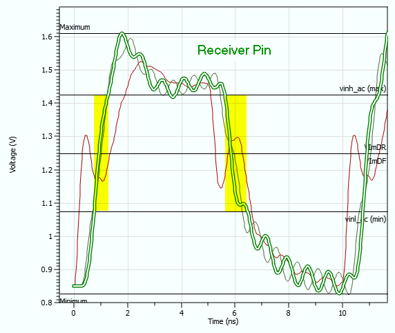
Conditions for the edge detection (Receiver)
For waveforms where suitable threshold values exist, such as Vinh_ac(max) and VIinl_ac(min), the waveform must cross both of these thresholds. Otherwise no edge is detected. An overshoot or undershoot, for example, is detected instead.
Specify the measured pulse number
In order to avoid an impact from any initial ringing on the obtained measurement results, you can specify the number of the pulse where the automatic measurement data is taken from the Simulator Options dialog. Where no threshold values are available, for example for differential pair curves, waveforms cannot be automatically measured by these methods. You can use a manual Point-to-Point measurement instead.
Extrema
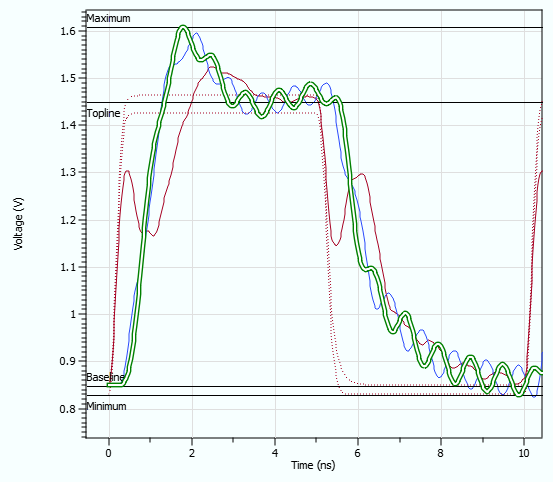
Measures the absolute maximum (Vmax) and minimum value (Vmin) of the selected waveform at the specified pulse. This is shown in the image in the Baseline section.
Topline
The topline voltage is derived by statistical methods on the selected waveform using a histogram. The higher main value of the histogram is used as the topline. In many cases this value is close to the static DC-High value of the circuit. This is shown in the image in the Baseline section.
Baseline
The baseline voltage is derived by statistical methods on the selected waveform, using an histogram. The lower main value of the histogram is used as the baseline. In many cases this value is close to the static DC-Low value of the circuit. This is shown in the following image.
1st /max Overshoot - Rising Edge
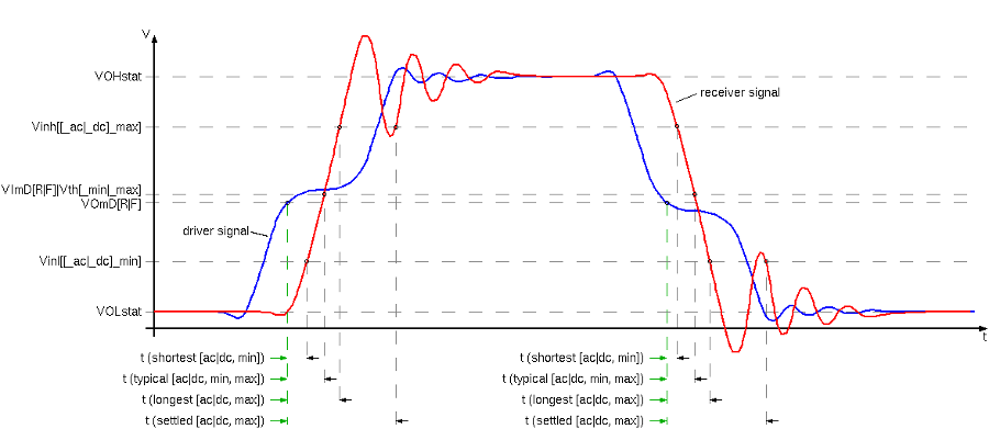
Defined as the first or maximum overshoot of the rising edge of the selected receiver signal, referring to the DC-High level. The reference voltage DC-High is computed by means of a DC-analysis of the circuit, with high output level of the driver or drivers. This is shown in the image in the 1st /max Undershoot - Falling Edge section.
1st /max Overshoot - Falling Edge
Defined similarly to the first or maximum overshoot - Rising Edge. The value is calculated as the overshoot considering the selected receiver signal, related to the DC-low level. The reference voltage DC-low is computed by means of a DC-analysis of the circuit with low output level of the driver or drivers. This is shown in the image in the 1st /max Undershoot - Falling Edge section.
1st /max Undershoot - Rising Edge
The first or maximum voltage of all undershoots of the selected receiver signal, for a rising edge. This is defined as 1./ Max. Undershoot (Rising Edge). This is shown in the image in the 1st /max Undershoot - Falling Edge section.
1st /max Undershoot - Falling Edge
The first or maximum voltage of all undershoots of the selected receiver signal, for a falling edge. This is defined as 1./ Max. Undershoot (Falling Edge) . This is shown in the following image.

Rise Time
Determines the 20% to 80% transition time of a rising edge. The percentages are relative to the difference (topline - baseline). The 10% to 90% rise time is also given.
Fall Time
Determines the transition time of a falling edge between 80% and 20%.The percentages are relative to the difference (topline - baseline). The 10% to 90% fall time is also given.
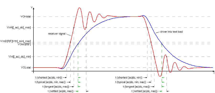
Flight Time
The Flight Time is always calculated between a receiver pin and a reference driver pin. See the notation in the following image. Which of these quantities is used depends on the availability of the thresholds in the IBIS model's Receiver Thresholds.
- "|" means one or the other value: "_ac|_dc". This means that either dynamic (ac) or static (dc) thresholds are used.
- [x] means that the variable "x" is optional: "Vinh[_max]". This means that either the Vinh or the Vinh_max threshold is used.
Compensated Flight Time
Another pin-to-pin interconnect delay is commonly defined as "Compensated Flight Time". This considers the driver's timing into a testload condition. The image below shows the threshold values used, and the derived compensated flight time measurements. These are for the rising and falling edge, respectively. The following notation is used. Which of these quantities is used depends on the availability of the thresholds in the IBIS model's Receiver Thresholds.
- "|" means one or the other value: "_ac|_dc". This means that either the dynamic (ac), or the static (dc) thresholds are used.
- [x] means that the variable "x" is optional: "Vinh[_max]". This means that either the Vinh or the Vinh_max threshold is used.
In order to derive the compensated flight time properly, a reference simulation
under test load conditions is performed. This is done on each simulation
of the electrical net, and may therefore take different possible packages
into account as well. The load condition is derived from the IBIS model,
if available. It is stored in the Simulation Model Library.
Test load parameters in IBIS are not mandatory. If no test load condition is present, then an open circuit is used as an alternative reference simulation.
The following image shows the test load condition as defined in the IBIS standard.
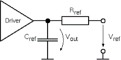
"The Cref and Rref subparameters correspond to the test load that the semiconductor vendor uses when specifying the propagation delay and/or output switching time of the model. The Vmeas subparameter is the reference voltage level that the semiconductor vendor uses for the model. Include Cref, Rref, Vref, and Vmeas information to facilitate board-level timing simulation."
For a better understanding, the following table lists the Zuken internal symbols and the IBIS ones. Since Zuken's Simulation Library incorporated most required values before they became part of IBIS, the terminology is slightly different. Also, Zuken's library is more precise and flexible in some cases. For example, in IBIS only a single measurement reference value (Vmeas) can be defined. In the Simulation Library it is possible to have different values for rising and falling edges, and inputs and outputs (V_OmD[RF], V_ImD[RF]).
| Zuken Symbol | IBIS Symbol | Comment |
|---|---|---|
| C_ref | Cref | Load capacitance |
| R_ref | Rref | Load resistance |
| V_ref | Vref | Termination voltage |
|
V_OHstat / V_OLstat |
Implicitly given in switching data |
Static high and low levels of the switching data |
|
V_OmDR / V_OmDF |
Vmeas Vmeas_rising Vmeas_falling |
Output reference voltage for delay measurements, Vmeas_rising, Vmeas_falling are part of Model_spec. |
|
V_ImDR / V_ImD |
Vref, Vth |
Input reference voltage Vref for delay measurements. Vref = (Vinh+Vinl)/2. Vth is part of Receiver Thresholds. |
The SI simulator returns the compensated flight time values, which are relative either to the reference waveform with test load, or to the reference waveform with no load.
There is no defined test waveform. The unloaded waveform (the response with no load) is used in its place for the compensated flight time measurements.
Flight Time Measurements in Differential Pairs
In differential pairs, the Flight Time measurement is more complex than in single ended E-Nets. For differential pairs with no differential termination, the Flight Times are derived between driver and receiver for the selected receiver pin of the differential pair. However, in cases where a termination connects the two halves of the differential pair, you will receive the flight time measurement results for the cross-over combination within the pair as well.
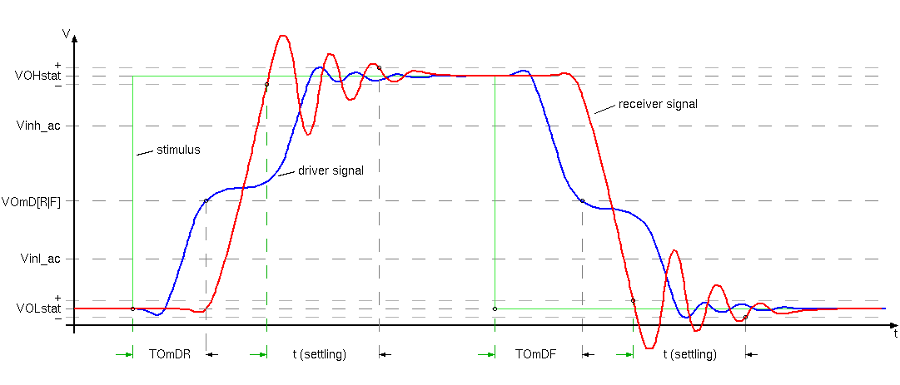
Settling Time
The settling time is defined between the time point at which the waveform reaches the span around the DC-high or DC-low level for the first time, and the time point where the waveform leaves the span for the last time. For the rising and falling edges, the span is defined as the value of the DC-High /DC-Low plus V_+ and minus V_-.
The values for V_+ and V_- are not calculated from the waveform. Instead, they are derived from the simulation model as follows.
+/- 10% of the static voltage range, between static high level V_OHstat and static low level V_OLstat:
span = +/- 0.1 * (V_OHstat-V_OLstat).
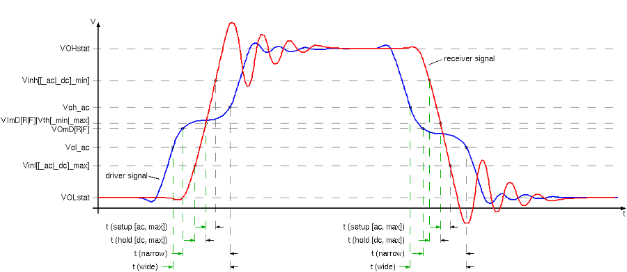
Slope
The Slope indicates how fast the transition is made between the low and high states of the signal at the receivers. A too long transition time might cause the buffer to fail switching, because the buffer internal comparator stage could fail to recognize the switching.
The Slope is defined as the time delay between the time points when the receiver signal first reaches the overdrive region, and the last time it leaves that region. It is measured independently for the rising and falling edge for both the driver and the receiver signal.
For the driver signal, Slope can be measured in the following ways, according to the JEDEC standards.
- Wide: between the dynamic thresholds Vol_ac and Voh_ac.
- Narrow: from the output reference voltage V_OmD[R|F] to the dynamic threshold Vol_ac (falling edge) / Voh_ac (rising edge).
- Vol_ac is defined as V_OmD[R|F] -20%
- Voh_ac is defined as V_OmD[R|F] +20%
For the receiver signal, the Slope is measured as follows.
- Setup: between the selected receiver's reference voltage and the dynamic threshold Vinl_ac (falling edge) / Vinh_ac (rising edge).
- Hold: between the static threshold Vinh_dc (falling edge) / Vinl_dc (rising edge) and the selected receiver's reference voltage.
In the following image:
- "|" means one or the other value: "_ac|_dc". This means that either dynamic (ac) or static (dc) thresholds are used.
- [x] means that the variable "x" is optional: "Vinh[_max]". This means that either the Vinh or the Vinh_max threshold is used.
Which of these quantities is used depends on the availability of the thresholds in the IBIS model's Receiver Thresholds.
Slew Rate
The Slew Rate is the ratio of the measured Slope value and the voltage differences. The values are typically provided in V/ns. These values are derived from the Slope measurements.
Eye Pattern Measurements
In SI Eye Pattern mode, various measurements are automatically performed on the time domain data. These measurement results are displayed in the Eye Pattern Measurements window. A detailed description of the Eye Pattern measurements is provided below.
Zero Level
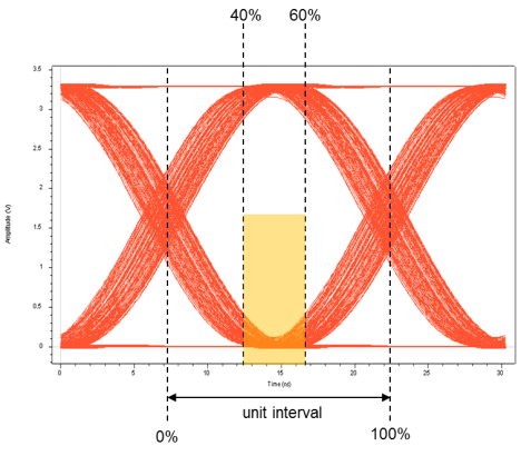
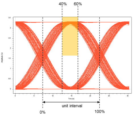
The EyeZeroLevel is the mean value of all data samples of a Logic Zero. For the computation of the Logic Zero level, all data samples are used in the range of 40% to 60% of the bit period, and in the lower half of the signal's amplitude.
One Level
The EyeOneLevel is the mean value of all data samples of a logic one. For the computation of the Logic One level, all data samples are used in the range of 40% to 60% of the bit period, and in the upper half of the signal's amplitude.
Amplitude
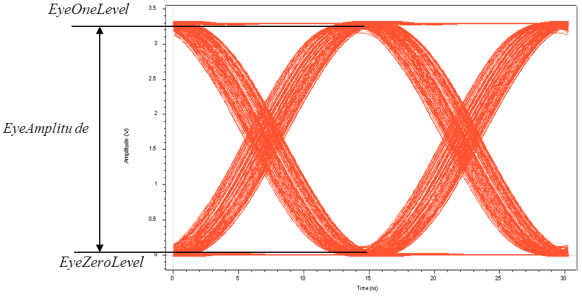
The Eye Amplitude is the difference between the EyeOneLevel and the EyeZeroLevel.
Height
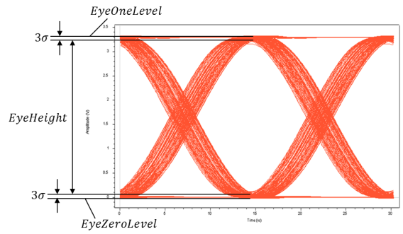
Eye height is a measure of the vertical opening of the eye pattern. An ideal eye opening measurement would be equal to the eye amplitude measurement. For a real eye diagram measurement, noise on the eye will cause the eye to close.
The eye height is defined as the 3s distance (standard deviation) between the two eye levels EyeOneLevel and EyeZeroLevel.

Width
Eye width is a measure of the horizontal opening of an eye diagram. The Eye Width is calculated from the two eye crossing points EyeCrossing@t1 and EyeCrossing@t2 values, and the root mean square deviation s. The two eye crossing points are determined by use of statistical methods on the eye pattern, and are also used for the auto-centering of the eye pattern.

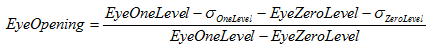
Opening Factor
The opening of the eye is calculated from the EyeOneLevel and EyeZeroLevel values, and the root mean square deviation s at zero level and one level.
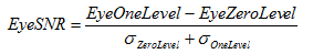
Signal to Noise Ratio (SNR)
The eye signal to noise ratio is calculated from the EyeOneLevel and EyeZeroLevel values, and the root mean square deviation s at zero level and one level.
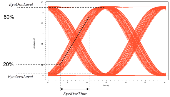
Rise Time
Eye rise time is a measure of the mean transition time of the data on the upward slope of an eye diagram. The measurement is typically made at the 20% and 80%, or the 10% and 90% levels of the slope. Both sets of values are available in SISS.
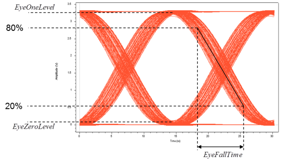
Fall Time
Eye fall time is a measure of the mean transition time of the data on the downward slope of an eye diagram. The measurement is typically made at the 20% and 80%, or the10% and 90% levels of the slope. Both sets of values are available in SISS.
Crossing Percentage
The crossing level is the mean value of a thin vertical histogram window, which is centered on the crossing point of the eye diagram.
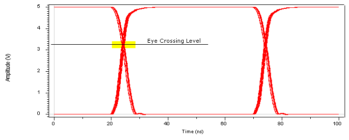
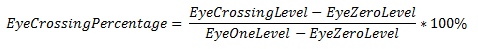
The EyeCrossingPercentage is calculated using the following equation.
The relative EyeCrossingPercentage gives an indication of duty cycle distortion or pulse symmetry problems for the high speed data signal.
- Eye crossing percentage is a measure for amplitude distortions caused by differences in the One Level and the Zero Level durations.
- When the EyeCrossingPercentage deviates from the perfect 50% point, the eye pattern closes and the transmission quality of the signal is degraded as a result.
Setup and Hold Measurements
Setup and hold times are important parameters when dealing with synchronous designs such as memory interfaces.
- Setup time is defined as the minimum amount of time before the clock's active edge arrives, in which the data must have settled for it to be latched correctly. A violation may cause incorrect data to be captured, which is known as setup violation.
- Hold time is defined as the minimum amount of time after the clock's active edge arrived, during which data must remain stable at the input pin. Violation in this case may cause incorrect data to be latched, which is known as a hold violation.
Define the clock signal in the Strobe Signal from the list of available signals and the data signal. Do this by choosing the Base Signal in the Working Set. The selected base signal is used to center the eye pattern. If no strobe signal is selected, then the setup and hold measurement is performed without considering the strobe's jitter. To calculate setup and hold times, first define a setup and hold mask in the Mask Editor. The parameter definition is shown in the image below.

The following steps are performed to calculate the Setup and Hold mask position and the margins.
- The jitter of the strobe signal is calculated at the defined voltage level V_REF.
- All time values of the strobe signal are considered at the voltage level V_REF, within the eye pattern of the base signal.
- The left most value and right most value are calculated. The difference between these values is the jitter of the strobe signal.
- If no strobe signal is selected, then the mask is centred in the eye pattern of the selected base signal. In this case the jitter value is zero.
- The setup mask is attached to the left bound of the jitter, and the hold mask is attached to the right bound of the jitter.
- The crossing points of the base signal with the voltage values V_IL(AC), V_IL(DC), V_IH(AC), V_IH(DC) are calculated.
- The margin is calculated from the crossing points of the base signal with the reference voltage values, and the end points of the Setup and Hold mask. The margin is the minimum value of the upper and the lower crossing of the reference values. If the mask width is larger than the eye opening, then no margin is available.
