
The PI/EMI Analysis module provides analysis capabilities for board-level EMI, Power Integrity and DC issues on circuit boards.
Launching PI/EMI Analysis
To launch PI/EMI Analysis, click PI/EMI Analysis on the Analysis tab in eCADSTAR. A new main window is opened. Existing PI/EMI analysis results can be opened by clicking Analysis > PI/EMI > PI/EMI Analysis Heatmap.The title of the main window shows the name of the analyzed design. Individual windows for the Classification, and the EMI and PI/DC data are shown within the main window. A comprehensive view of all relevant data is provided by the various analysis algorithms.
- Additional information which is needed for the analysis can be entered, and edited in the Classification dialog.
- Analysis-specific settings and PI/EMI analysis results are provided in the following dialogs:
Details are provided in separate tabs, depending on the type of analysis results.
- A Log dialog lists relevant information on the progress of the analysis.
- Menus provide access to various functions of the PI/EMI Analysis module.
- Shortcuts allow quick access to many functions.
- Toolbars provide frequently-used functions, and can be arranged as required.
- The status bar shows any issues with the data or with the EMC behavior of the design.
An Options dialog allows you to control GUI and analysis-related settings. These are stored either on a per-user basis, or on a per-design project basis where the analysis results are affected by a settings.
A progress dialog shows the progress of the calculations, per algorithm.
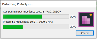
The progress of sub-tasks is shown using a secondary progress bar, where appropriate. The Cancel button allows you to abort most of the longer running tasks. In some cases it is not possible to directly terminate an operation. In these cases, the progress dialog shows an appropriate message.
To avoid producing an inconsistent set of data, the classification process cannot be stopped.
Menus
The following menus are provided in PI/EMI Analysis. These allows you to launch the analysis for EMI, DC and Power Integrity. They also allow you to control the analysis and display options, and configure export options. Commonly-used commands are also provided on separate Toolbars.
File Menu
| Value | Description |
|---|---|
 Open Open
|
A file selection dialog is opened allows you to open a PI/EMI enhanced RIF file (*.erf or *.rif). If another design is still open and any unsaved changes exist, then a confirmation dialog is displayed. Click Save to save any changes. Alternatively, click Cancel to cancel the operation or click Discard to discard the changes. |
| Recent Files | Displays the ten most recently-opened design files in PI/EMI Analysis. |
 Close Close
|
Removes the current design data from PI/EMI Analysis. The PI/EMI Analysis module remains open, and allows you to open another design. If there are unsaved changes, then a confirmation dialog is displayed. Click Save to save the changes. Alternatively, click Cancel to cancel the operation or click Discard to discard the changes. |
 Save Save
|
Saves the settings specified in the Options
dialog and the changes made in the Classification
and Power Bus dialogs. The classification
data is stored in the .ecf file in
the following directory: [design_name].emc\[design_name].ecf. Note Table results are not stored automatically. To ensure consistency between design data and the results, re-run the analysis if you relaunch PI/EMI Analysis module. |
 Options Options
|
Displays the Options dialog for PI/EMI Analysis. This allows you to set the control parameters for the EMC analysis. |
 Export CSV Export CSV
|
Displays the Export CSV dialog. This
allows you to export all results and classification data to CSV
files. Individual files are generated for the following.
|
 Quit Quit
|
Closes the PI/EMI Analysis module. If a design is still open and unsaved changes exist, then a confirmation dialog is displayed. Click Save to save the changes. Alternatively, click Cancel to cancel the operation or click Discard to discard the changes. |
Edit Menu
Tools Menu
| Value | Description | |
|---|---|---|
| Starts the classification of the design data. This button is made available when classification is required. This process includes pre-processing steps which are required for analysis. This may require significant computation time, depending on the size of the design data. Data includes the number of nets, components, supply systems, etc. Some manual changes of the classification data will require this action, and in order to ensure data-consistency, some tables will not be editable. If all classification is consistent, and current, then this button is made unavailable. The classification data is saved in the .ecf file. For further information, see the Options dialog, Classification tab. | ||
 Open PCB design Open PCB design
|
The design on which the analysis is performed in the PI/EMI Analysis module is displayed in eCADSTAR PCB Editor. | |
 Manage Simulation Library Manage Simulation Library
|
Launches the Simulation Library Manager . This allows you to manage Devices, Models and Packages for SI, PI and EMI Analysis in the eCADSTAR Analysis Module. | |
 Reload Simulation Library Reload Simulation Library
|
If the simulation library is updated while the PI/EMI Analysis module is running, then clicking Reload Simulation Library will reload it. If there are unsaved changes in the PI/EMI Analysis module, then you are prompted to save them. | |
| Check Supply Pin Type Definition | Launch the Supply Pin Type Report dialog which displays a list of undefined, but potential supply pins. See Supply Pin Type Report. | |
 EMI Analysis EMI Analysis
|
Performs the PI/EMI Analysis using the settings in the Classification and Power Bus dialogs. When completed, the Radiation dialog is displayed. This dialog shows the EMI-related results of the analysis which are caused by the signal currents on the electrical nets. The results are separated into various tabs, depending on the coupling path from the source (signal current) to the antenna, and on the different parasitic antenna types. The EMI Analysis command is made available when you change a setting in the Classification or Power Bus dialog. | |
| CM Voltage Distribution | Allows you to display the Common Mode Voltage Distribution of
the board, on the canvas in eCADSTAR PCB Editor.
Select from the following options on the displayed sub menu. The
PI/EMI
Analysis Heatmap dialog is launched.
Note
|
|
| Common Mode Voltage Map | If specified, then the Common Mode Voltage distribution across the board is displayed on the canvas in eCADSTAR PCB Editor. The common mode voltage distribution is typically a frequency-dependent property of the design. For simplicity, the distribution with the largest common mode voltage is displayed automatically. | |
| Selected | If specified, then you can select at which frequency the voltage map is displayed. Select a frequency in the CM Voltage Distribution - Selected dialog, and click Plot. The list of frequencies is created from all the clock frequencies and their respective harmonics of the signals in your design. The clock frequencies are defined in the Classification dialog, Net table. | |
 I/O Coupled
Voltage Distribution I/O Coupled
Voltage Distribution
|
Allows you to display the I/O Coupled Voltage Distribution for one or more selected I/O signals on the canvas in eCADSTAR PCB Editor. The same functionality is available on the assist menu in the Radiation dialog for selected I/O signals. | |
 PI Analysis PI Analysis
|
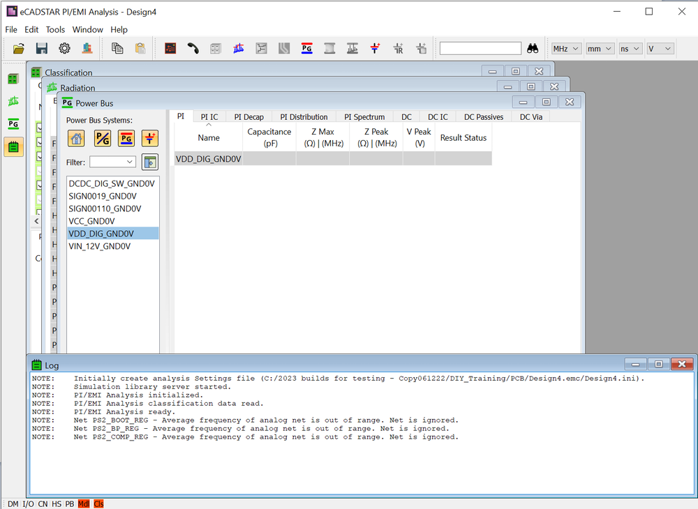
Performs PI Analysis on selected supply systems. The Power Bus dialog is displayed. If a supply system is not selected, then this command is made unavailable. If any input data that is relevant to PI has been changed, then the PI algorithm is executed and the results are updated in the Power Bus dialog. If all results are current, then the PI Analysis button is made unavailable. This command can also be executed from the context menu for a selected power bus. | |
 Impedance
distribution Impedance
distribution
|
Allows you to calculate the Impedance
distribution Z(x,y) within the power/ground plane pairs of
the selected supply system. The respective PI Distribution tab in the Power Bus dialog allows you to specify the relevant frequency. If a frequency is not selected, then this command is made unavailable.
|
|
 Impedance
spectrum at position Impedance
spectrum at position
|
Allows you to calculate the Impedance
spectrum Z(f) at position (x,y)within power/ground plane pairs
of a selected supply system. The respective PI
Spectrum tab in the Power
Bus dialog allows you to specify the relevant position. If
no location is specified, then this command is made unavailable.
|
|
 DC Analysis DC Analysis
|
Executes DC Analysis. If any input data that is relevant to DC has been changed, then the DC algorithm is executed and the results are updated in the Power Bus dialog, DC tab. If all results are current, then this button is made unavailable. You can also execute this command from the Power Bus tree view by selecting it on the assist menu, for a selected power bus. To send the DC result maps to the canvas in eCADSTAR PCB Editor, select Voltage/Current Distribution on the assist menu. | |
 DC-R
Extraction DC-R
Extraction
|
Executes the DC-R
Analysis. The DC-R Extraction command calculates the DC resistance
values between individual supply pins of ICs. It does this by
considering each IC source pin in turn, and calculating a separate
resistance value for each IC load pin. Every source-load combination
will therefore have a calculated resistance value. If no DC-Analysis
has been run on a supply system, then this button is made unavailable.
|
|
 Voltage/Current
Distribution Voltage/Current
Distribution
|
Sends the DC result maps to the canvas in eCADSTAR PCB Editor. Alternatively, select Voltage/Current Distribution on the assist menu in the DC tab in the Power Bus dialog. The DC Analysis command must be executed before you execute this command. | |
| All Analysis | Launches the EMI, PI and DC Analysis simultaneously. Alternatively, press Ctrl+Alt+A. | |
 Send Selection Send Selection
|
For items that you select in any of the PI/EMI Analysis module dialogs, click Send Selection to highlight it on the canvas in eCADSTAR PCB Editor. Alternatively, press Ctrl+B. |

Window Menu
The Window menu
allows you to specify window settings, and launch the PI/EMI
Analysis dialogs.
| Value | Description |
|---|---|
| Cascade | Arranges the PI/EMI Analysis dialogs in a predefined cascade style. |
| Tile | Arranges the PI/EMI Analysis dialogs in a predefined tiled style. |
| Store Layout | Saves the layout of the PI/EMI Analysis dialogs. This allows you to restore the layout by clicking Restore Layout. |
| Restore Layout | Restores a previously-saved layout of the PI/EMI Analysis dialogs. |
 Classification Classification
|
Displays the Classification dialog in the PI/EMI Analysis module. The tabs of the Classification dialog allow you to enter all the required data for EMC analysis. Much of this may already be supplied by the system. |
 Radiation Radiation
|
Displays the Radiation dialog in the PI/EMI Analysis module. The Radiation dialog shows emissions for which signal currents and voltages are the primary source. Depending on the antenna coupling path, the results are separated into the following tabs: EMI Net, EMI Connector, EMI Heatsink, EMI Power Bus and EMI Frequency. The EMI Frequency tab summarizes all emission results of the individual radiation mechanisms and antenna coupling paths. This allows you to easily locate the source of a problem at a certain frequency. |
 Power Bus Power Bus
|
Displays the Power Bus dialog in the PI/EMI Analysis module. The Power Bus dialog shows information related to the power supply systems and shows issues associated with switching currents. |
 Log Log
|
Displays the Log dialog in the PI/EMI Analysis module. |
You can also launch a PI/EMI Analysis dialog from the Window toolbar, or by using a shortcut key.
Help Menu
| Value | Description |
|---|---|
 Help Help
|
Displays the Online Help. This is also displayed by pressing the F1 key. |
 Release Number Release Number
|
Displays the version of eCADSTAR, and copyright information. |
Shortcuts
The following shortcuts are available in the PI/EMI Analysis module dialog.
Toolbars
The toolbars allow you to launch frequently-used commands.
File Toolbar
| Value | Description |
|---|---|
|
Open design file |
See Open in the section above. |
|
Save settings and classification |
See Save in the section above. |
|
Options |
See Options in the section above. |
|
Export analysis results and classification in CSV |
See Export CSV in the section above. |
Edit Toolbar
| Value | Description |
|---|---|
 Copy Copy
|
See Copy in the section above. |
 Paste
Paste
|
See Paste in the section above. |
Tools Toolbar

| Value | Description |
|---|---|
|
Open associated PCB design
|
Opens the associated design in PCB Editor. See Open PCB Design. |
|
Send Selection
|
Highlights the selected item on the canvas in eCADSTAR PCB Editor. See Send Selection. |
| Starts the classification of the design data. See: Classification. | |
| Execute EMI
Analysis
|
Starts the EMI Analysis. See: EMI Analysis. |
 Common Mode Voltage Map (Requires EMI Analysis) Common Mode Voltage Map (Requires EMI Analysis)
|
If specified, then the Common Mode Voltage distribution across the board is displayed on the canvas in eCADSTAR PCB Editor. See: Common Mode Voltage Map. |
| Display I/O
Coupled Voltage Distribution Map for Selected Signals
|
Allows you to display the I/O Coupled Voltage Distribution for one or more selected I/O signals on the canvas in eCADSTAR PCB Editor. See: I/O Coupled Voltage Distribution. |
| Execute PI Analysis
|
Performs PI Analysis on selected supply systems. The Power Bus dialog is displayed. See: PI Analysis. |
| Generate
Impedance Distribution Map for Selected Frequencies (requires
PI Analysis)
|
Allows you to calculate the Impedance distribution Z(x,y) within the power/ground plane pairs of a selected supply system. See: Impedance Distribution. |
| Generate
Impedance Spectrum Map for Selected for Selected Positions (requires
PI Analysis)
|
Allows you to calculate the Impedance spectrum Z(f) at position (x,y) within power/ground plane pairs of a selected supply system. See: Impedance Distribution Position. |
| Execute DC Analysis
|
Executes DC analysis. See: DC Analysis. |
| Extract DC-R
from DC Analysis (requires DC Analysis)
|
Executes the DC-R Analysis. See: DC-R Extraction. |
| Display
DC Analysis Result Maps (requires DC Analysis)
|
Sends the calculated DC result maps to the canvas in eCADSTAR PCB Editor. See: Voltage/Current Distribution. |
Search Toolbar

The Search command
allows you to locate an item in a selected view, such as a component,
a net within an E-Net or the E-Net itself. For example, you may want to
view all components that are connected to a selected power bus, such as
ICs or Decaps. To achieve this, select the Net
tab in the Classification dialog,
and then enter a supply net. Press Enter
or click ![]() . The relevant net is highlighted
in the Net table. All related components in
the other dialogs are also selected automatically if they are associated
with the selected net.
. The relevant net is highlighted
in the Net table. All related components in
the other dialogs are also selected automatically if they are associated
with the selected net.
Units Toolbar
The Units toolbar allows you to easily change the units for the columns and information windows. Toggle the display of this toolbar using the Display Units Tool Bar check box in the Options dialog.
Window Toolbar
The Window toolbar allows you to display the following PI/EMI Analysis Module dialogs.
| Value | Description |
|---|---|
|
Classification |
Displays the Classification dialog. For an overview, see: Classification. |
|
Radiation |
Displays the Radiation dialog. For an overview, see: Radiation. |
|
Power Bus
|
Displays the Power Bus dialog. For an overview, see: Power Bus. |
| Log
|
Displays the Log
dialog contains important messages. For example, relating
to potential problems with the layout data.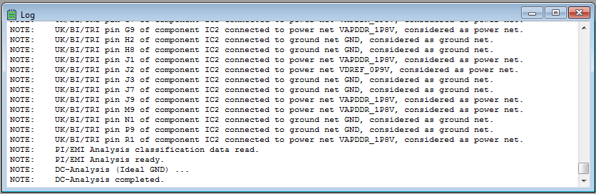 |
Status Indicators
The status bar at the bottom of the PI/EMI Analysis module window shows the following status indicators:
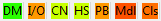
These allows you to easily identify problems with the design or data.
The first five indicators show green, yellow or red levels of emissions for a specific EMC effect. These change their status when a given threshold is passed. The thresholds are given in dB (V/m).
- The threshold for yellow is 50dB (V/m) and above.
- The threshold for red is 70dB (V/m) and above.
- The initial state of these indicators is unset, and the color is white. If a specific EMC effect does not apply to your design, then the color stays in white. This might occur if no connector is present, and hence there is no I/O-coupling.
- The Mdl and Cls indicators have a continuous color between red and green.
| Value | Description |
|---|---|
| DM | Shows the status of differential mode emission. |
| I/O | Shows the status of emission due to I/O-coupling. |
| CN | Shows whether cables attached at connectors act as antenna for current-driven common mode emission. |
| HS | Shows whether heatsinks, mounted on ICs act as antenna for current-driven common mode emission. |
| PB | Shows the status of emissions caused by PowerBus noise. |
| Mdl | Shows the status of I/O buffer models that are available at IC pins. |
| Cls | Classification settings are not set to default for Net type, Clock frequency, and Rise and Fall times. |
Options Dialog
The Options dialog in the PI/EMI
Analysis module allows you to set control parameters for EMC analysis.
Launch this dialog by clicking File > Options
on the toolbar in the PI/EMI Analysis module.
Alternatively, click  on the
toolbar. The settings specified in this dialog are stored in the following
locations.
on the
toolbar. The settings specified in this dialog are stored in the following
locations.
- All Analysis-related settings which may affect the accuracy of results are stored with the design in the project directory. The file location is: [design_name].emc\[design_name].ini.
- All settings related to the interface, which do not affect the analysis results, are stored separately for each user in a system ini file in the installation folder. The file location is: [install_dir]\Analysis\setting\pia.ini. These settings include units, the number of decimal places, scaling, colors etc. The pia-analysis.ini file is also in this location. This file contains initial values for the analysis-related settings. Its content is copied into each new project. This separation provides consistent results for different users.
In the descriptions of individual settings in this topic, the following definitions apply.
- "User setting" indicates the storage within the system ini file.
- "Project setting" refers to a design-specific setting.
- Do not modify the .ini files manually.
- In a new design with no project settings, default values are applied that are taken from the pia-analysis.ini file.
The following tabs in the Options dialog are described below.
General Tab
The General tab allows you to define the following options in the PI/EMI Analysis module.
| Value | Description | |
|---|---|---|
| Number of Decimal Places | Allows you to set the number of decimal places that are displayed in the PI/EMI Analysis module dialogs. | |
| Units | Allows you to set the units that are displayed in the PI/EMI Analysis module dialogs, and on the toolbar. | |
| Display Units Tool Bar | If selected, then the Units toolbar is displayed in the PI/EMI Analysis module. | |
| Display Cell Button | Allows you to specify whether buttons are displayed in the PI/EMI Analysis module tables when you point the cursor in a relevant cell. Regardless of this setting, all relevant commands can be accessed by right-clicking a cell and selecting the option on the assist menu. You can also specify the functionality of the buttons that are displayed when you point the cursor in relevant table cells. These settings are applied immediately when you click OK in the Options dialog. | |
| Selected | Buttons are displayed in the PI/EMI Analysis module tables when you point the cursor in a relevant cell. The Preferred Action field is made available. | |
| Not Selected | Buttons are not displayed in the PI/EMI Analysis module tables when you point the cursor in a relevant cell. The Preferred Action field is made unavailable. | |
| Preferred Action | Allows you to specify the functionality of the buttons that are displayed when you point the cursor in relevant table cells, in the PI/EMI Analysis module table. This field is made available when you select Display Cell Button. | |
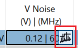
| Spectrum | If spectral results are available, then this button is shown
in all result columns in the Radiation
and Power Bus dialogs when you
point the cursor in them. If no spectral results are available,
for example because no spectrum has been computed, then the button
for the Info dialog is displayed instead. The spectral result
plot can also be displayed by right-clicking the cell and selecting
this option on the assist menu.
|
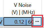
|
| Dialog | The button for the Info dialog is displayed for the relevant
cell when you point the cursor in it. The Info dialog can also
be displayed by right-clicking the cell and selecting this option
on the assist menu.
|
|
| Automatic CSV Export | Provides settings to automatically write result data to CSV formatted files when a DC, EMI or PI analysis is performed. The CSV Export can either use fixed formatting options or the formatting options from the CSV export dialog, dependent on the settings in the CSV Format Options. The automatic CSV Export is available for:
Note To store the automatically exported CSV files for longer use, you must copy them elsewhere, especially if the Remove Result on Design Close is selected. |
|
| Tables | By enabling this check-box the respective result tables are exported into CSV files upon completion of an analysis.
The export is done regardless of the selected data in the Export CSV dialog.
The target export folder is fixed to <design_name>.emc\export to avoid any conflicts with intentionally selected folder in the manual CSV Export. Note The automatically exported classification tables always correspond to the last performed analysis, regardless of the analysis type (EMI, PI, or DC). There is no distinction in DC-, PI-, or EMI classification. |
|
| Spectral Plots | By enabling this check-box any opened spectral plot shown in the Analysis Result Viewer is exported into an corresponding CSV file.
The radiation view related files are stored in the EMI sub directory of the <design>.emc folder. The powerbus view related files are stored under the <design>.emc/PI/<Powerbus> folder. For each element (IC, signal, position, …) a single file is generated with the name of the element. The prefixes are the same as used for the ARV export. Note All combined plots, e.g. TotalE, Parallel Circuit, etc. are omitted from the CSV export. |
|
| CSV Format Options | Choose the formatting options to be either Fixed, or as in Export CSV Dialog. The Fixed formatting options are:
|
|
| Remove Results on Design Close | If selected, then all PI and DC results files in their respective folders, are deleted when the PI/EMI Analysis Module is closed. This may help to reduce the used disk space. |
Classification Tab
The Classification tab allows you to control the automatic classification process for net type recognition, and the color coding in the Classification dialog.
Supply Net Recognition
| Value | Description |
|---|---|
| Analyse Active Supply Systems, only | If selected, then PI and DC results are only provided for supply net pairs to which active components (ICs) are connected. For example, "VCC" and "GND_D". Otherwise, all combinations of power and ground nets are displayed. This may result in a longer list of supply systems. |
| by Power Pin | If selected, then you can automatically assign the net type Supply to a net, if the net is connected to a power supply pin for the device. This setting can be viewed and edited in the Simulation Library Manager, Digital IC Editor. |
| by Ground Pin | If selected, then you can automatically assign the net type Supply to a net, if the net is connected to a ground supply pin for the device. This setting can be viewed and edited in the Simulation Library Manager, Digital IC Editor. |
| by Name | If selected, then automatic supply net recognition is used. This derives the signal type and supply voltage from the signal name, and is case insensitive. For example, "VCC", "3V3" or "GND". For details, see Supply Net recognition in the Net Classification section. |
| Auto Connect | If selected, then supply nets are combined across series passive components when loading the design data into the PI/EMI Analysis module. The DC resistance value must be lower or equal to the value in the Auto Connect Resistance Limit box. You can view and edit these connections in the Connect Nets dialog. |
| Auto Connect Resistance Limit | If Auto Connect is selected, then specify a value in this box. Supply nets are combined across series passive components when loading the design data into PI/EMI Analysis Module. The DC resistance value is lower or equal to the value that you specify. |
Analogue Net recognition
| Value | Description |
|---|---|
| by Transistors | If selected, then nets are automatically classified as analog if the E-Net is connected to a Transistor. You can change the E-Net type in the Net tab in the Classification dialog. This is a Project Setting. |
| by Series Capacitors | If selected, then nets are automatically classified as analog if the E-Net includes series capacitors. You can change the E-Net type in the Net tab in the Classification dialog. This is a Project Setting. |
| by Series Diodes | If selected, then nets are automatically classified as analog if the E-Net includes series diodes. You can change the E-Net type in the Net tab in the Classification dialog. This is a Project Setting. |
Colors
This section allows you to modify the color coding in the Classification dialog. These are User settings.
| Value | Description |
|---|---|
| Default Setting | Allows you to specify a color to default values, initially red. This is applied if no other value is set. |
| User Setting | Allows you to specify a color for user defined values, initially yellow. This is applied if a value has been manually set. |
| System/Library Setting | Allows you to specify a color to System values, initially green. This value is derived from the PI/EMI Analysis module, or from the Simulation Library content. |
| Reset | Resets the color values to the initial settings. |
Analysis Tab
The Analysis tab allows you to control some geometrical limits which impact the PI and EMI Analysis. If you change any of the settings, then the input data must be added again. All of these settings are Project related.
| Value | Description | |
|---|---|---|
| E-Net Settings | The E-Net Settings section allows you to control the following E-Net parameters. | |
| Min E-Net Length | Electrical nets with a total length that is less than the minimum E-Net length are ignored in the EMI Analysis. The default value is 5.000mm. | |
| Max Segment Length | Individual track segments in a net are sub-divided into smaller sub-segments, if they have a segment length that is larger than the maximum segment length. This provides higher accuracy, but results in a slightly higher calculation time. Most EMI algorithms work on segments, or sub-segments where available, as a single entity to be analyzed. The default value is 2.000cm. | |
| Conductor Settings | Allows you to control the precision for copper shape handling. | |
| Min Copper Area | Copper shapes that have a smaller area than the minimal copper
area are ignored in the analysis. For example, a return path.
The default area is 1e-6mm².
Note This setting only applies in PI Analysis. It is not applied in DC Analysis. |
|
| Min Cutout Area | Cutouts that are smaller than the minimal cutout size are ignored in the analysis. The default cutout area is 1e-6mm². | |
| Via Settings | Gives control over the default Via model used within the DC-Analysis. If required, individually adjust the values in the Classification dialog, Via Type tab table for each Via Type. |
|
| Plating Thickness | This is the default value for the Plating Thickness of Vias.
When the value is set to 0.0, a filled Via is used. |
|
| Plating Conductivity | This is the default value for the Plating Conductivity of Vias. When the value is set to 0.0, an average value of the Layer conductivities is used. These are listed in the Classification dialog Layer tab. |
|
| Parallel Processing |
Note
Parallel Processing allows you to execute numerically intense algorithms in parallel on multiple CPU cores. This applies to the DC Analysis and some suitable PI algorithms.This functionality is currently unavailable. |
|
| Number of Threads | Define the maximal number of parallel threads. The largest allowed value is derived from your actual CPU data, usually considering hyper-threading. As more threads are used, the run time may be reduced. However, the memory demand (RAM) is increased. A good compromise between speed and increased memory usage is to limit the number of threads to the number of actual physical CPU cores, not using hyper-threading. Note An example of DC Analysis is provided below.The possible gain from using this option may be limited by the PC system performance (I/O to disk and memory), and the structures that are analyzed.
|

EMI Tab
| Value | Description | |
|---|---|---|
| Distance of Antenna | Allows you to control the distance of the receiving antenna,
which measures the electric field strength. As the EMI algorithms
only target far field effects, you can enter values that are equal
to or larger than 3m. The default value is 3m. This is a Project
Setting. Note The results of radiated field strength in the PI/EMI Analysis module dialogs are updated immediately. However, spectral plots must be re-opened to obtain the corresponding field values. |
|
| Common Mode Voltage Map | Allows you to control the resolution of the computed map file
using a slider bar. The grid size for the Common
Mode Voltage map is automatically adjusted, depending on
the board's dimensions.
Note
|
|
| Resolution | Allows you to set the resolution using the slider bar. The
resolution is doubled in each step.
If you change this setting, then the EMI Algorithm must be executed again. Existing results are removed from the results dialogs. The default position is the second step from left. This results in a grid size between 4mm and 8mm. This is a Project setting. |
PI Tab
Frequency Range
Allows you to define the frequency range of the PI Analysis between specified From and To values. The maximum frequency is 10GHz. The minimum start frequency is 100kHz. You can either specify logarithmic or linear frequency stepping. These are Project Settings.
The computation time is determined by the number of frequency steps within the given frequency range.
| Value | Description | |
|---|---|---|
| From | Allows you to define the lower value of the frequency range for the PI-Analysis. | |
| To | Allows you to define the upper value of the frequency range for the PI-Analysis. | |
| Logarithmic | Logarithmic stepping defines the number of frequency steps per decade. This allows a relatively small number of frequencies, even over a wide frequency range. | |
| Number per decade | Specify the number of frequency steps per decade. | |
| Linear | Linear stepping defines a fixed equidistant frequency step across the full frequency range. Specify this value in the Step box. | |
| Step | Allows you to specify the fixed equidistant frequency step across the full frequency range. |
Impedance Calculation
| Value | Description | |
|---|---|---|
| Grid Size | Allows you to control the accuracy and run-time of the numerical algorithm for the impedance calculation of power/ground plane pairs. This value sets the grid size in which the power plane pairs are discretized. It is used as a starting value within the grid, which can be further controlled using theCoarsening Levelfield. This is a Project Setting.Larger, mostly uniform overlap areas may not need to be discretized into small cells, but can be computed using a wider mesh. In such cases, the grid size may become larger.Connecting components such as ICs and decaps, as well as boundaries to other overlap areas or cutouts will enforce the smallest grid size, according to the entered value. | |
| Coarsening Level | For the impedance calculation of power/ground plane pairs,
this setting allows you to control the accuracy and the run-time
of the numerical algorithm. It controls how often the mesh in
the Grid Size box can be doubled.
A Coarsening Level of "0" will create a mesh with a
uniform grid size. If you specify a Grid Size of 1mm and a Coarsening
Level of 5, then the mesh will become more coarse in the following
five steps, if possible: 2 mm, 4 mm, 8 mm, 16 mm and 32 mm. These
grid sizes are applied where possible. For example, in areas where
large overlap areas exist and there are no cutouts, or where connecting
components are present. This is a Project setting.
|
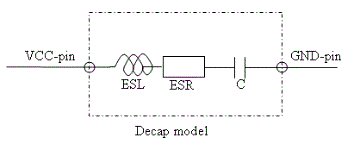
RF Circuit Decaps
Allows you to specify the default value for an equivalent R-L-C circuit to be used to model. For example, decoupling capacitors in the Power Integrity (PI) Analysis in this area. This value must be larger than or equal to zero. The same circuit model is applied for ICs and Connectors as loads within the PI-Analysis. This is done in order to improve the model accuracy without assigning specific (SPICE) circuit models for decoupling capacitor (decaps) in Constraint Browser.
| Value | Description | |
|---|---|---|
| Effective Series Resistance | The Effective Series Resistance is indicated by the ESR symbol in the above image. | |
| Effective Series Inductance | The Effective Series Inductance is indicated by the ESL symbol in the above image. | |
| C in | The capacitance is indicated by the C symbol in the above image. | |
| Use Package Based ESL/ESR values for Decaps | If selected, then package based ESR and ESL values can be used
for decaps. These values can be customized. When a design is loaded,
the available package model data are read from an XML file. The
default file is located here: [install_path]|eCADSTAR
{version}\Analysis\settings\smdPackages.xml. This file contains some commonly-used SMD package types, with their correspondent ESL/ESR values. Alternatively, you can provide your own package types by providing an SMD package XML file at the following location: APPDATA\Roaming\Zuken\eCADSTAR {version}\Analysis\settings\smdPackages.xml. This takes precedence over the system one, if it exists. This configuration file contains the following values for every supported package.
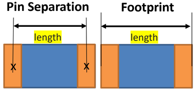
The ESR and ESL values may vary with the capacitance, but can also be given independently of the capacitance. The applied package can be identified based on the Pin Separation or by the Footprint data available in the layout data. The Footprint data are often more reliable in actual design data than measuring the Pin Separation. However, the different footprints may vary between the top and bottom layer for the same component. The length is derived as shown in the images below.
Width and thickness are not considered, and are therefore not contained in the XML definition for the package type. Review the package type in the PI Decap table where the Parasitic Model column shows the recognized size. You can manually overwrite these pre-set values in the Power Bus dialog for each IC or decap. These settings are Project Settings. If this check box is selected, then the Derive Package from field is made available. |
|
| Derive Package from | Allows you to specify the method used to identify the package size. This setting is only available if Use Package Based ESL/ESR Values for Decaps is selected. If you change this setting, then the design data are evaluated again for all decaps when you click OK. | |
| Pin Separation | The package size is identified according to the distance between the pins positions in the layout data. | |
| Footprint | The package size is identified, based on the footprint size. This method is not recommended if a design uses a different footprint on each side of the board for the same part. |
RF Circuit ICs
| Value | Description |
|---|---|
| Effective Series Resistance | Specify the default series resistance value for an equivalent R-L-C circuit to be used to model the input circuit of IC power pins for Power Integrity (PI) Analysis. This value must be larger than or equal to zero. |
| Effective Series Inductance | Specify the default series inductance value for an equivalent R-L-C circuit to be used to model the input circuit of IC power pins for Power Integrity (PI) Analysis. This value must be larger than or equal to zero. |
| C in | Specify the capacitance value for an equivalent R-L-C circuit to be used to model the input circuit of IC power pins for Power Integrity (PI) Analysis. This value must be larger than or equal to zero. |
| Use Open Circuit IC Models |
Allows you to apply an open circuit model for ICs. This replaces the RLC-model that is defined in RF Circuit. These are Project settings. Note This setting changes all IC models at the same time. For individual IC settings, use the RLC-model parameter. For example, by using a zero value capacitance. |
RF Circuit VRMs
This functionality is currently unavailable.
| Value | Description |
|---|---|
| Effective Series Resistance | Specify the default series resistance value for an equivalent R-L circuit to be used to model the voltage regulator modules (VRMs) for Power Integrity (PI) Analysis. This value must be larger than or equal to zero. This is a Project setting. |
| Effective Series Inductance | Specify the default series inductance value for an equivalent R-L circuit to be used to model the voltage regulator modules (VRMs) for Power Integrity (PI) Analysis. This value must be larger than or equal to zero. This is a Project setting. |
DC Tab
Grid Size
Allows you to set the grid size in which supply planes are meshed, between minimum and maximum values. This allows you to control the accuracy and run-time of the numerical algorithm for the DC-calculation of supply planes. The actual grid size of a copper shape is in this range, but is controlled by geometrical parameters for each plane, individually. This, and all other DC Analysis settings are Project settings.
| Value | Description |
|---|---|
| Min Grid Size | Set the minimum grid size in which supply planes are meshed. |
| Max Grid Size | Set the maximum grid size in which supply planes are meshed. |
Power System
Allows you to specify that a numerical analysis of power planes is included for DC-Analysis. This estimation is based on the copper resistance of a large plane. It considers the true distance of the connection points to the plane, but not the actual shape.
| Value | Description |
|---|---|
| Include Power Planes | If selected, then the DC Analysis includes a numerical analysis of power planes. Otherwise, estimated values for the resistances of the power planes are used. |
Ground System
In situations where the Ground system is not present in a design, these settings allow you to perform a DC-Analysis of the power system.
| Value | Description |
|---|---|
| Ideal Ground | If selected, then you can perform DC-Analysis with an ideal ground system. This may provide a good initial insight into the DC behavior of the design. |
| Include Ground Planes | If selected, then the DC-Analysis includes a numerical analysis of ground planes. Otherwise, estimated values are used for the resistances of the ground planes. This estimation is based on the copper resistance of a large plane. The true distance of the connection points to the plane is considered, but not the actual shape. |
DC-R Extraction
Allows you to specify whether IC-internal connections are considered in the DC-R Extraction.
| Value | Description |
|---|---|
| Connect Pins across Package Resistors | If selected, then the power pins within one group are considered
to be connected across the IC-internal package resistors. This
may significantly change the overall DC-network due to additional
parallel paths across typically low resistances. Hence the pin-to-pin
resistance values will change accordingly. If not selected, then
all internal IC circuitry is ignored for the DC-R Extraction,
and the pure interconnect is considered. |
Exporting Results Data
The Export CSV command allows you to export
the data from the PI/EMI Analysis module result
views to CSV formatted files after the analysis is complete. Launch this dialog by clicking File
>  Export CSV on the toolbar in the PI/EMI
Analysis module.
Export CSV on the toolbar in the PI/EMI
Analysis module.
Alternatively, click on the toolbar.
The Log dialog is updated to show
whether the export was successful. The exported CSV (Comma Separated Values Format) files use the system-defined
coding table on your operating system to format value sequences, such as "Unicode UTF-8",
or a Japanese character set. This is selected automatically.
| Value | Description | |
|---|---|---|
| Folder | Displays the path to the exported CSV file. | |
| Browse | Allows you to specify a folder to export the CSV file to. Select the folder in the displayed dialog. | |
| Select data for export | Allows you to specify the results data that is exported by
selecting the relevant check boxes. The data is exported to the
following individual CSV files. Note If a particular analysis has not been performed, then the associated check box is made unavailable. For example, performing EMI Analysis in the PI/EMI Analysis module makes the EMI Radiation and EMI Frequency check boxes available. |
|
| EMI Radiation | If applicable, the following EMI-related results are exported
from the data in the Radiation
dialog.
|
|
| EMI Frequency | The following EMI-related frequency results are exported.
|
|
| Power Bus PI | The following PI-related results are exported from the data
in the Power Bus dialog.
|
|
| Power Bus DC | The following DC-related results are exported from the Power
Bus dialog.
|
|
| Classification | The classification data in the individual Classification dialogs are exported as follows. All data is exported, rather than just manually-entered data. Exporting all Classification data also ensures consistency. There is no indication of the source of the data as the cell colors are not exported. Individual files are created for the following views. Component Classification: CLASS_Component.csv Component Classification with sub-tables for Pin: CLASS_Component_Pin.csv Layer Classification: CLASS_Layer.csv Net Classification: CLASS_Net.csv Supply Net Classification: CLASS_Supply.csv Via Classification: CLASS_ViaType.csv | |
| CSV Format Options | This section allows you to specify the formatting of the exported CSV file. | |
| Separator | Specify the delimiter that is used in the exported CSV file.
This setting is saved in the user settings. The following options
can be selected.
|
|
| Extended Header | Allows you to exclude additional header information such as
the creation date and version information. This may be necessary
to avoid it corrupting the import function in your target applications.
|
|
| Values as shown in GUI | Allows you to specify whether all values are exported in base
units.
|
- The I/O coupling report combines the information into one table. It contains a list of all I/O nets and their biggest coupled aggressors.
- The file is created in parallel to the EMI result table files with the name EMI_Net_IO_Coupling_Results.csv.
- The report is created on the manual and the automatic CSV export as part of the EMI Radiation export.
Supply Pin Type Report
When loading a design in the PI/EMI Analysis tool, the Supply Pin Type Report dialog is displayed with a list of undefined, but potential supply pins. If it is has been closed, it can be launch by using the Check Supply Pin Type Definition option in the Tools Menu. See the section on Setting up the Supply System for background information on this check and why it is needed.
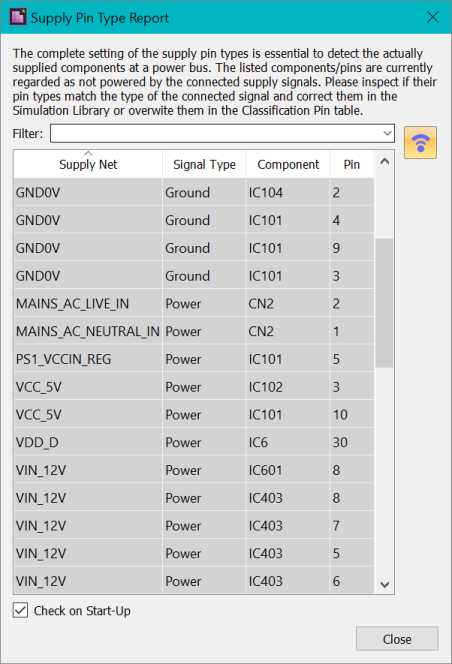
The Supply Pin Type Report dialog lists the pins of IC's and connectors which do not have expected connections to the power and/or ground nets. This dialog allows you to specify pin types when loading designs.
- Selecting the pins in the report highlights the correspondent pins in the classification pin table. By default this is done automatically. If this automatic highlight becomes too slow (on huge designs) it can be turned off by clicking on the
 Toggle Immediate Highlight button. Then use the assist menu to manually highlight selected pin.
 - A check report is listing all those ICs and connectors which do not have any supply pin definition at all. For these components the supply net, its type, the component and pin name are listed.
- Use the Filter field to reduce the number of listed pins, e.g. by Component name or Signal Type.
- Select one or a group of pins. These pins are automatically highlighted in the Classification dialog, Component tab, Pin table.
- Set the Pin Type in the Pin table to POWER or GROUND.
The pin type check can be run when loading a design into the PI/EMI Analysis tool. This can be disabled by turning off the check box Check on Start-Up.
The pin type can also be set in the Classification dialog, Component tab, Pin table.
