
The main purpose of the DC-Analysis tool is to check whether the supply voltage levels at the active component’s power pins are acceptable, or whether a voltage drop occurs somewhere in the supply system, which is too high. These DC-Analysis results are presented in the DC tables in the Power Bus dialog in the PI/EMI Analysis Module. In addition, a detailed list of DC resistance values between all IC power pins can be obtained by executing the DC-R Extraction method. The resistance values are listed in the DC and DC-IC tab when the computation method is completed.
Identification of Supply Systems
Similar to PI Analysis, the correct definition of the supply systems is required before you can execute DC Analysis. At the start, the PI/EMI Analysis Module distinguishes the supply nets into groups of Power and Ground type nets. This is based on net attributes, but also by interpretation of the net name. Names like "GND", "VCC" and "3.3V" are recognized. However, any setting made in the design system or in Constraint Manager is preferred.
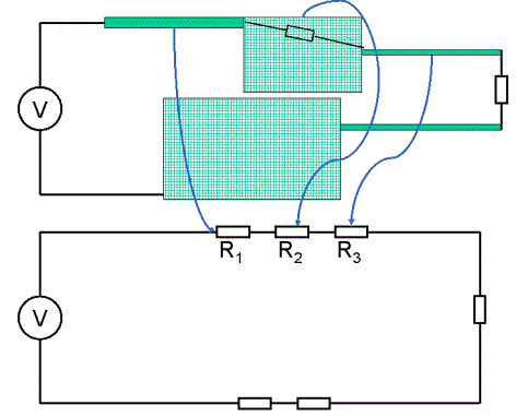
If the power net is made up from two or more power nets that are connected together by passive components, then the Connect Nets dialogue can be used to indicate that there is a connection. The same consideration applies for ground nets. For more details, see: Power Integrity Analysis: Supply Systems. All combinations of Power and Ground supply system pairs are identified to which ICs or Decaps are connected. Those combinations with no further components attached to the pair are not considered valid power busses. All others are considered at a later stage, and will be listed in the Power Bus dialog.
How to Configure the DC Analysis
To obtain results from DC Analysis, one active device (IC or connector) must be configured as a source, and one or more loads is required. This can be done on a per-pin basis in the DC IC tab of the Power Bus view. This also allows the package resistance and minimum voltage to be specified. All these devices must connect to both the power net and the ground net. These connections can be direct or through a passive component.
If this list is empty or if some ICs are missing, then the PI/EMI Analysis Module has probably failed to recognise them as ICs. You can check this in the Component tab of the Classification dialog. ICs are identified as "IC" in the Type column.
You can configure analysis settings in the DC tab of the Options dialog.
DC Algorithm
DC Analysis comprises the following three major processing steps.
- DC-Plane Characterization
- DC-Network Analysis
- DC-Distribution Construction
DC Network Set-up
The DC Network is a complex electric circuit that is only composed of resistors.
In order to build this network, all elements belonging to a Power Bus must be converted into equivalent resistances, and inserted into the DC Network at the appropriate locations. In order to set up the DC Network, the data stored in the ERF and CTF files are mapped into the internal data structures when the PI/EMI Analysis Module is launched. If errors or problems are encountered during the DC Network setup, then appropriate messages are displayed. The individual element types are handled as follows.
Tracks and Vias
For all track segments and vias of a Power Bus, the required resistances are determined from the geometry and conductivity information with the help of analytical formulas. The copper thickness, conductivity, and track-width or via-thickness, respectively, are considered, as well as the length of the track/via-element. For vias, each layer transition is considered separately.
Copper Planes
In order to set up a complete equivalent DC Network, the planes are replaced by a set of equivalent resistances, one for each contact-to-contact pair. Since the values for the plane equivalent resistances cannot be computed directly, approximate values are used at this stage. The approximation is computed with an analytical formula that is based on the assumption of an infinitely large plane, and vanishingly small contact points. The values for these equivalent resistances are determined more precisely during the first step of the DC Analysis Computation. The approximated resistance values for the planes used at this step are physically meaningful. These serve as fallback values if computational problems occur during the analysis of the plane.
Resistors, Inductors and Capacitors.
Within this process stage, passive components are added to the DC Network. Resistors are introduced into the DC Network directly, by value. If the resistance value is zero, then the following two cases are distinguished.
- Serial connection: the SHORT circuit value of 1µΩ is inserted.
- Shunt connection between power and ground: the OPEN circuit value of 1MΩ is inserted.
Inductors are replaced by the SHORT circuit value of 1µΩ.
Capacitors, with the exception of shunt elements between
the power and the ground net, are replaced by the OPEN circuit value of
1MΩ.
The shunt capacitors are not inserted into the DC Network, and are therefore
ignored by the DC Analysis computation. This is because they do not affect
the flow of current.
Power Consuming ICs and Connectors.
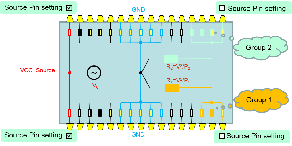
Active components (ICs) are modeled by their power consumption. This can be specified in the DC IC tab of the Power Bus dialog. This power consumption value is transferred into a resistor as R0=V²/P, which is inserted into the DC-Network. Alternatively, the current consumption can be specified as well.
Also, the IC’s bond-wires are modeled as small resistors. These connect the power consumption resistor R0 with the grouped pins of the active component. Connectors are handled here in the same way as ICs.
Source Component
From the list of the ICs and connectors of the supply system, one can be selected to act as the driving source for the DC Analysis. The IC-internal connections are also considered in the source component.
If needed, a pin-based source setting is available. Only selected power pins will drive the DC circuit with the voltage source. The remaining power pins act as power consuming loads. These are defined by their power consumption setting.
Groups of source pins can be defined. The source pins within a group are internally connected through the bond-wire resistors. This means that the outside circuitry is near to short-circuited by these resistors. The effect of this IC internal connection can be observed in the results of the DC-R Extraction. This can be executed either with or without the bond-wire resistors in place. Different groups may have an individual power consumption. In order to avoid the internal connection, the relevant source pins must be ungrouped. These settings can be made in the DC IC table.
DC Analysis Computation
Although the DC Network is completed during the DC Network setup, and can already be analyzed, the initial resistances for the planes are estimated values. These are based on idealizing assumptions. In order to provide a more accurate equivalent resistance, the planes are characterized by a numerical method.
DC Plane Characterization
In this step, all supply copper planes are analyzed individually with respect to the contact-to-contact resistance. This copper plane analysis is a key area of the analysis, and requires a large portion of the overall computational effort. This is particularly true with large and complex copper shapes. The runtime also depends on the number of contacts to the individual planes.
In this step, the copper shapes are meshed into square cells, which have a well defined edge-to-edge resistance. All these equivalent resistance values are connected and hence form a large electrical network. The solution time for this network strongly depends on the number of grid cells, and on the type of the solver used.
A finer mesh requires more computational effort in terms of CPU time and memory consumption. However, a certain step size for the mesh should not be exceeded. If it is exceeded, then the accuracy is compromised when the resolution of the geometrical features becomes poor. The meshing itself is done in an automatic process. This is controlled by the following user settings in the Options dialog: Min Grid Size and Max Grid Size. Within these boundaries, the meshing algorithm automatically determines a suitable cell size for each copper shape. This depends on the geometric properties of the current copper shape.
DC-Network Analysis
This second step of the DC Analysis computation essentially performs two tasks. Initially, the resistance values of the planes that where initially approximated are replaced by the numerically-determined values that are computed during the DC Plane characterization. When this is established, the network is analyzed subject to the driving conditions given by the source component. The voltage drops are computed at all resistances.
DC Distribution Construction
When the voltage drops along the equivalent resistances are known, these voltage drops can be mapped onto the planes. Serving as a set of equivalent sources, the voltage and current distributions is constructed in each plane of the Power Bus.
DC Result Display
DC Analysis results are shown in the DC tables in the Power Bus view. Also, graphical results can be visualized. The respective results files are written to the directory <design_name>.emc\DC\.
