
The Constraint Browser Options dialog allows you to modify the behavior of Constraint Browser, and specify default settings for eCADSTAR PCB Editor. In Constraint Browser, it is displayed by clicking Utility > Options on the main menu. In eCADSTAR PCB Viewer, it is displayed by clicking Utility > Options on the Constraint Viewer main menu. When launched from eCADSTAR PCB Viewer, this dialog is named Constraint Viewer Options.
In Constraint Browser for eCADSTAR Schematic Editor or eCADSTAR Schematic Viewer, the Constraint Browser Options dialog is displayed. This dialog contains only the Receive action section. The setting that you specify applies only to eCADSTAR Schematic Editor.
Auto-Generated Net Labels
| Value | Description |
|---|---|
| Default Prefix | Specify the prefix for the net name that is used when you create a new E-Net in Constraint Browser for eCADSTAR PCB Editor. The default value is "SIGN". |
Delay, Characteristic Impedance, Differential Impedance
This section allows you to control the extraction of information from the design data. It is only available in a High Speed environment.
| Value | Description | |
|---|---|---|
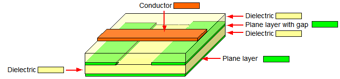
| Enable Enhanced plane extraction | Allows you to specify whether the true shape of a power or
ground reference plane is considered. As a result, the information
that is extracted form the design data is more granular. This
would consider cut-outs in clearance lands and thermal lands,
and would allow you to set a minimum segment length that is associated
with gaps on the reference plane. These values are used for calculating
delay or characteristic impedance. The following image shows a
conductor crossing a gap on a reference plane.
|
|
| Selected | The true shape of the reference plane is considered. The fields in this section are made available. If the reference plane does not exist, then a dummy reference plane is used. | |
| Not selected | The true shape of the reference plane is not considered, and it is treated as a powerplane (the layer attribute is set to Powerplane). If there is no powerplane layer, then a layer with the layer type set to Power or Ground is treated as a reference plane. The layer type of Power or Ground must be set for two or more layers. | |
| Include cut-out figure of clearance land and thermal land | Allows you to specify whether cut-out areas for clearance lands and thermal lands are considered for the reference plane. This field is made available if Enable enhanced plane extraction is set to ON. | |
| Selected | Cut-out areas are considered for clearance lands and thermal lands on the reference plane. | |
| Not selected | Cut-out areas are not considered for clearance lands and thermal lands on the reference plane. | |
| Min. segment length (mm) | If Enable enhanced plane extraction
is set to ON, then this field
is made available. A signal line is divided into segments, which
are created according to the size of the gaps in the reference
plane. Specifying a smaller value provides more granular data
for calculating delay and characteristic impedance. If a gap in
the reference plane is narrower than the Minimum
segment length value, then the gap is ignored and single
segment is extracted. If the gap is wider than this value, then
it is extracted as an additional segment. This is illustrated
below.
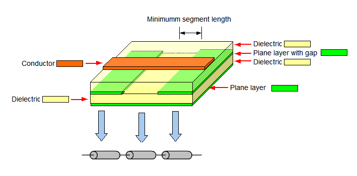 Note For separate areas of copper on a reference layer, the Minimum segment length value is ignored if a track passes over the gap between them. An additional segment is extracted regardless of whether the gap is wider than this value. |
|
| Coupling distance (mm) | Specifies the maximum distance between track segments for them to be considered coupled. The track segment on the selected net, and a track segment on an adjacent net are considered. If the angle between the track and the selected signal is less than 45 degrees, the tracks are considered parallel. | |
| Differential rule tolerance (%) | For the track width and track spacing of differential pair rule stacks, specify the acceptable tolerance as a percentage. This is the amount that these values vary from the Track Width and Track Spacing values that you specify for differential pair rule stacks in the Rule Editor Dialog: Differential Pairs Tab. | |
| Detect coupling at corners of Differential Pairs | For differential pairs, this setting allows you to specify whether the corners of a coupled segment is regarded as a part of the coupling. | |
| Selected | For differential pairs, the corner of the coupled segment is regarded as a part of the coupling. | |
| Not Selected | For differential pairs, the corner of the coupled segment is not regarded as a part of the coupling. |
Send action
When pin pairs are cross probed from Constraint Browser or Constraint Viewer in eCADSTAR PCB Editor or eCADSTAR Schematic Editor, this section allows you to specify whether they are selected or highlighted.
| Value | Description | |
|---|---|---|
| Select pin pair | When pin pairs are cross probed from Constraint Browser or Constraint Viewer in eCADSTAR PCB Editor or eCADSTAR Schematic Editor, they are selected. | |
| Highlight pin pair | When pin pairs are cross probed from Constraint Browser or Constraint Viewer in eCADSTAR PCB Editor or eCADSTAR Schematic Editor, they are highlighted. | |
| Blink | Allows you to specify that highlighted pin pairs blink when
they are cross probed from Constraint
Browser or Constraint Viewer
in eCADSTAR PCB Editor
or eCADSTAR Schematic Editor.
|
Receive action
When nets are cross probed to Constraint Browser or Constraint Viewer in eCADSTAR PCB Editor, this section allows you to specify whether the associated E-Net or just the net is selected. To specify this setting in eCADSTAR Schematic Editor, see: eCADSTAR Schematic Editor: Constraint Browser Options.
| Value | Description |
|---|---|
| Select signal | When a net is cross probed to Constraint Browser or Constraint Viewer from the canvas, the associated E-Net is selected, rather than the net. |
| Select net | When a net is cross probed to Constraint Browser or Constraint Viewer from the canvas, only the net is selected, rather than the associated E-Net. |
Probe location
Allows you to set the probe location priorities for timing and SI measurements.
| Value | Description |
|---|---|
| Refer to Simulation library manager | Measurement is done according to the probe location settings for each device in the Simulation Library Manager. If measurement fails at the die position, then the pin position is used. |
| Pin | Measurement is done at the pin position. |
| Die | Measurement is done at the die position. If measurement fails at the die position, then the pin position is used. |
