
When you select a pad from the library and associate it with a footprint layer in a padstack, you control how it is used by modifying the settings shown below. You can specify these settings in the Padstack Editor dialog.
| Value | Description |
|---|---|
| Padstack Name | The name of the padstack within the library. |
| Layer | A selected footprint layer to which pads can be assigned. |
| Connected PadUnconnected PadThermal PadClearance Pad | Selected pads that you can set on selected Footprint Layers.
Connected, unconnected, thermal and clearance pads can all be
set on the same footprint layer.
Note Thermal pads and clearance pads are used with a power plane when post processing as a negative artwork. They are also used with positive/negative layer types. |
| Drill Diameter | The diameter of drill for drilled padstacks that penetrate multiple layers. Where there is no drill hole, this value must be set to zero. |
| Slot Length | Where the aperture is a slot, this is the slot length in currently-set units. |
| Slot Orientation | Where the aperture is a slot, this is the angle of the slot in degrees relative to reference axis. |
| Plated | This indicates that the drill hole is plated. |
| Multiple Layer Contact | This is set when the padstack makes contact on multiple conductor layers. For example, when the padstack is referenced by through-hole pins or vias. In some situations, a padstack can make contact with multiple layers even if there is no drill hole. |
| Build-Up Via | Indicates that the padstack is a build-up via. Build-up vias are differentiated from vias that penetrate core layers. |
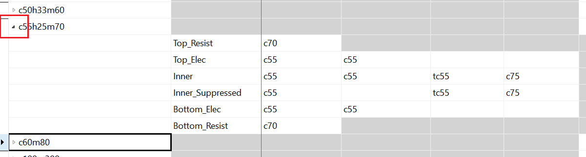
Note
- Most of the fields in the Padstack
Editor dialog, described above, cannot be edited. To access the
layer, connected pad, unconnected pad, thermal pad or clearance pad,
you may have to expand the padstack by clicking the arrow shown below.
- Consider the following when connecting to padstacks in eCADSTAR PCB Editor.
- If a padstack contains no connected or unconnected pads and no hole, then you cannot connect to it in eCADSTAR PCB Editor. A padstack that only contains holes will always cause DRC errors.
- If a connected, unconnected, thermal or clearance pad is defined, then a pad is always displayed.
- In negative areas, if neither thermal nor clearance pads are present, then connections can still be made. However, DRC errors will occur due to short-circuits (usually to planes).
