
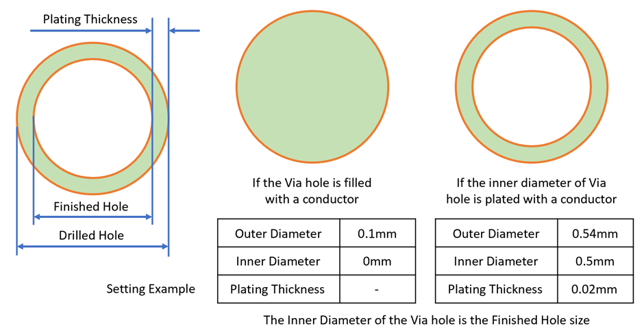
Configuring Vias
This topic explains how to configure via settings. The following image shows the configuration of two types of via.
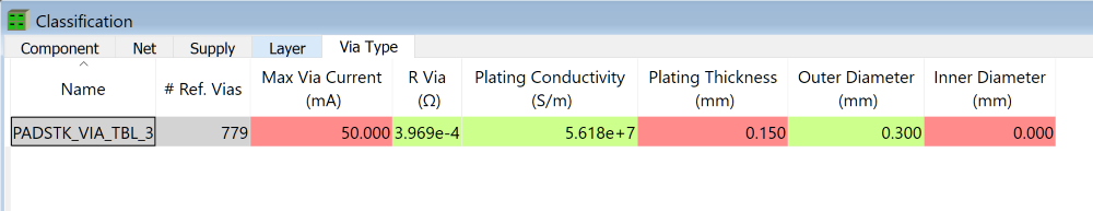
- In the eCADSTAR PI/EMI Analysis module, Classification view, select the Via Type tab. All the via types in the design are listed.
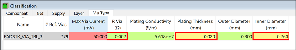
- Enter "0.020" in the Plating Thickness column of PADSTK_VIA_TBL_3. The via resistance and inner diameter are automatically calculated, and the R Via and Inner Diameter values are updated.
Note
You can check the via resistance value more easily by changing the units to mW in the Options dialog.
You can check the via resistance value more easily by changing the units to mW in the Options dialog.
